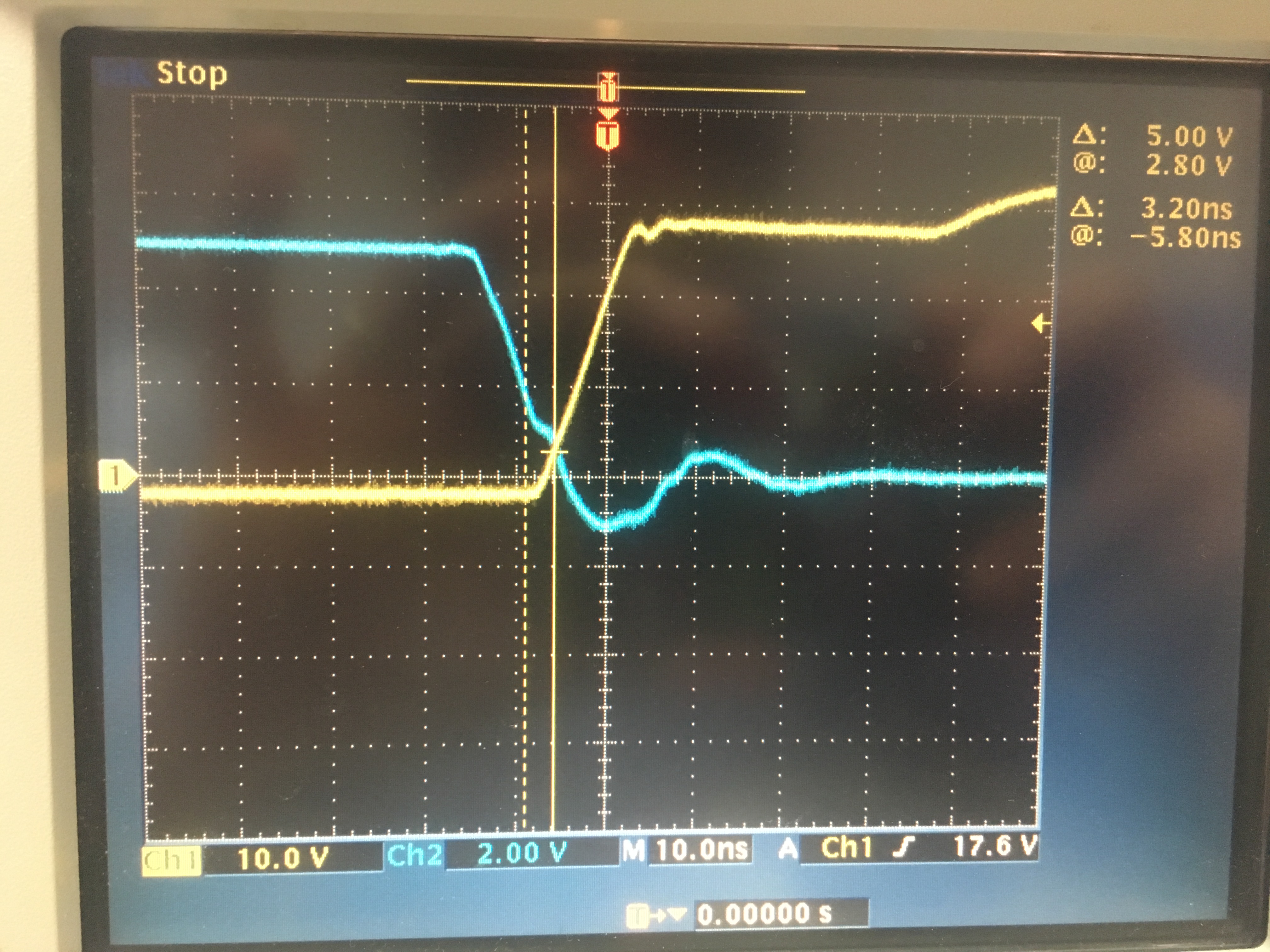
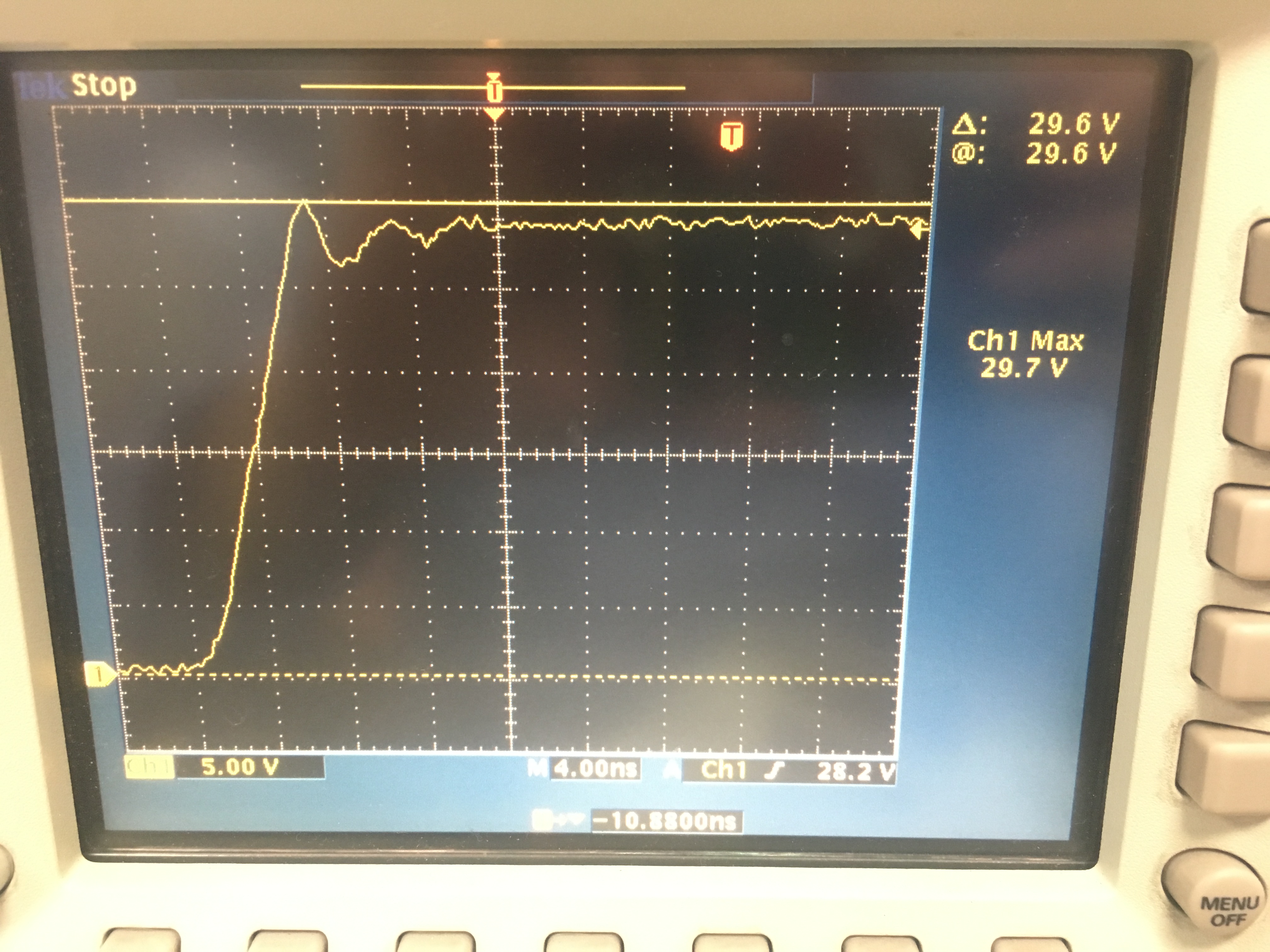
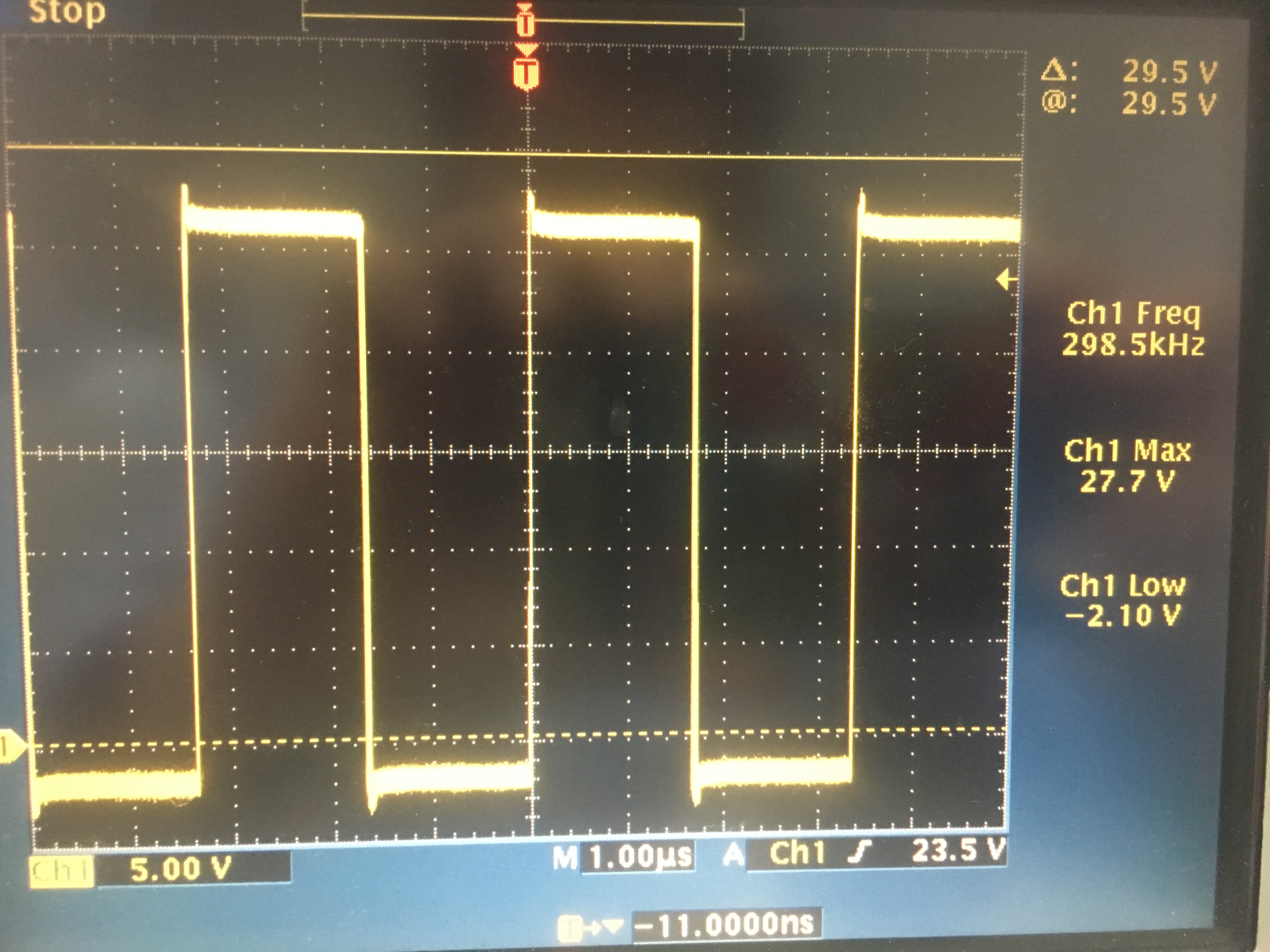
Dear Team,
Please kindly help to confirm where my schematic needs to be modified, as +12V and +5V output phase low-side MOSFET(Q38&Q8) is always damaged.
what is the most likely cause of damage?
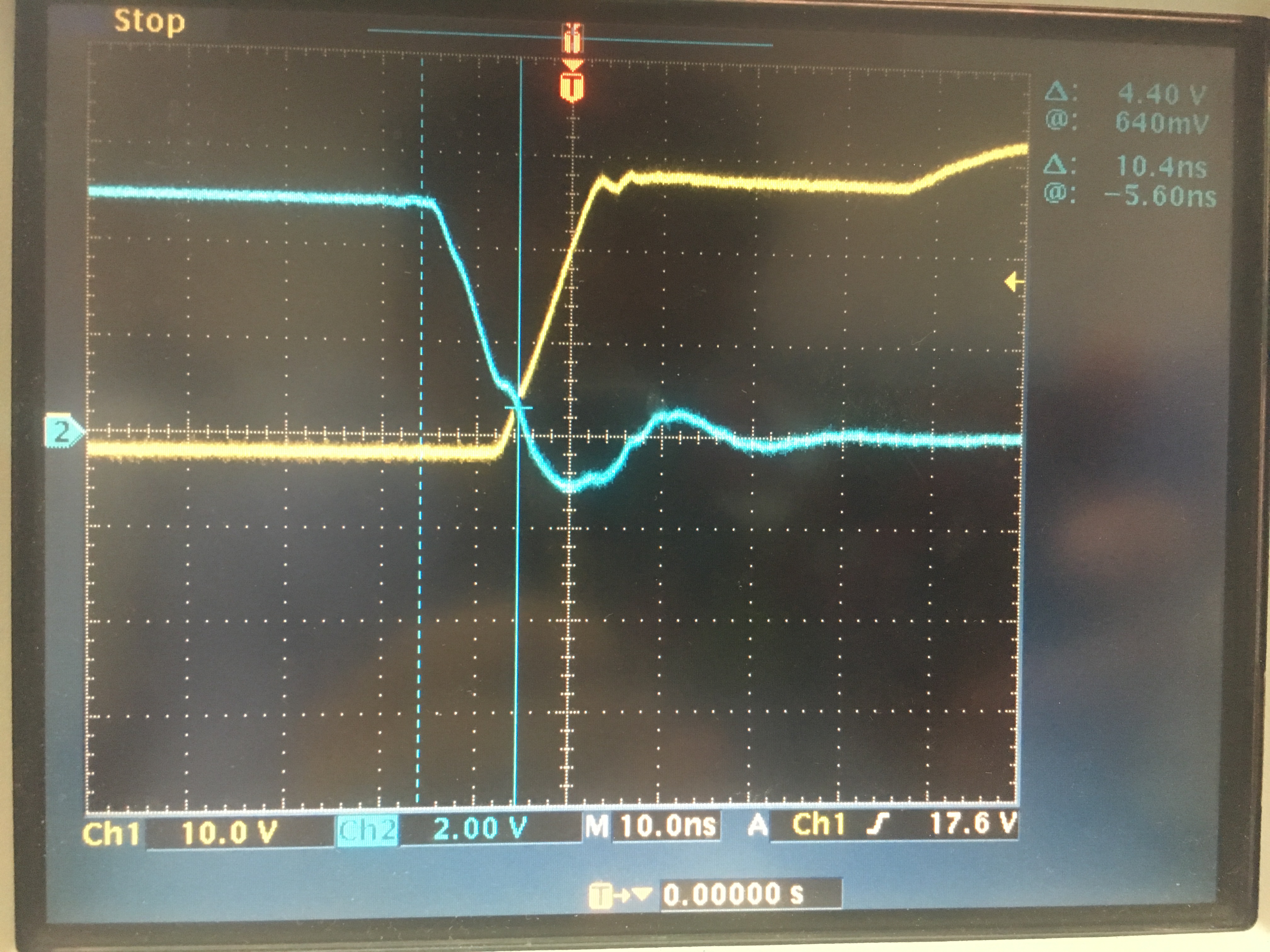
Dear Team,
Please kindly help to confirm where my schematic needs to be modified, as +12V and +5V output phase low-side MOSFET(Q38&Q8) is always damaged.
what is the most likely cause of damage?