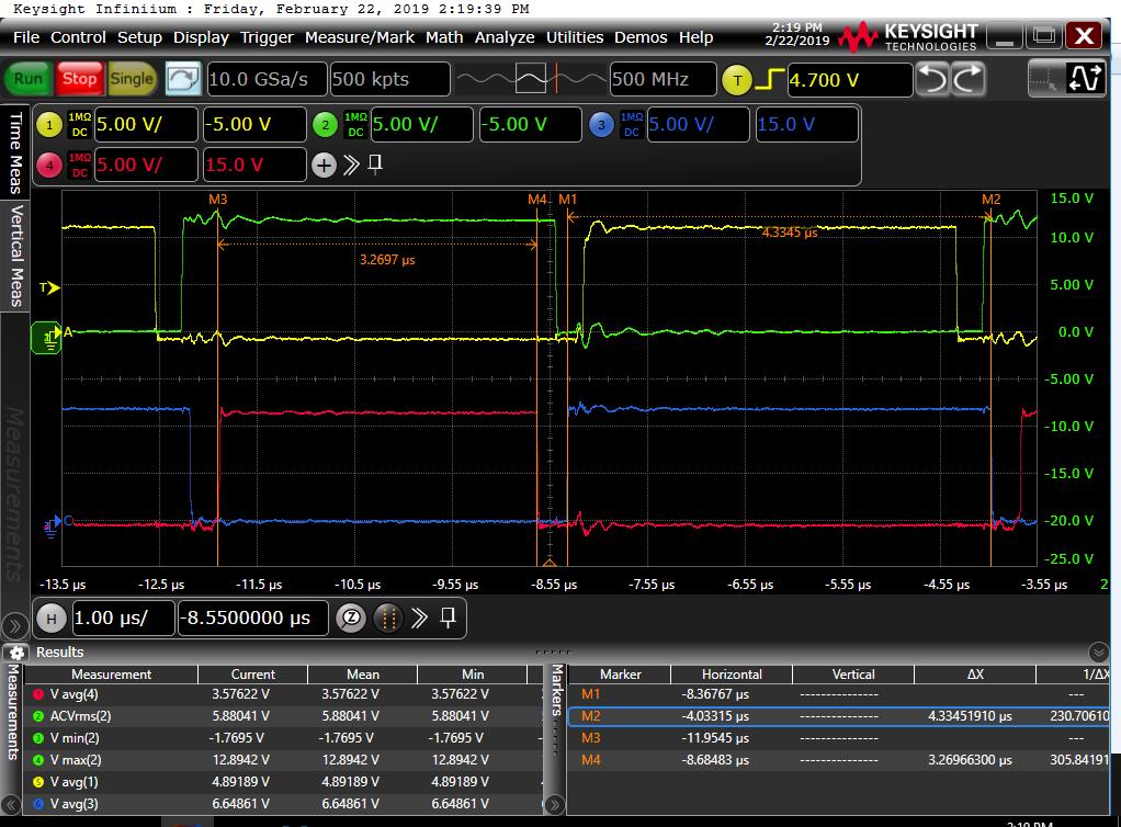
This thread has been locked.

If you have a related question, please click the "Ask a related question" button in the top right corner. The newly created question will be automatically linked to this question.

UCC28950: UCC28950 : On Time of OUTC and OUTD changes.

Part Number: UCC28950
Hi.

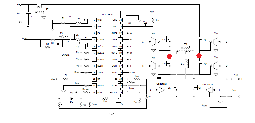
I am using UCC28950.

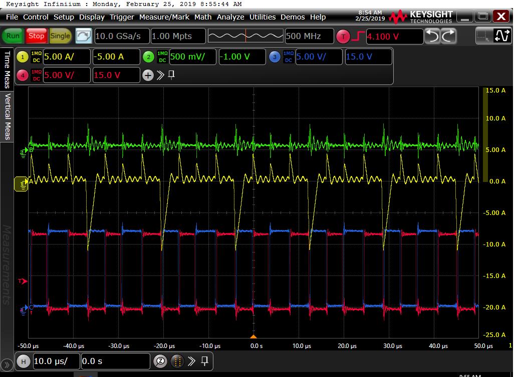
The ontimes of the outputs OUTC and OUTD of UCC28950 change.

As far as I know, PhaseShift thinks that the ON and OFF times should always be the same (assuming DeadTime is 0).

However, the ON OFF Time of OUTC and OUTD changes depending on the output load.
(1 cycle is 8us, and the ON time changes from 3.2us to 4.2us.)

On the other hand, OUTA and OUTB always maintain constant ON time.

Is it normal for the ontimes of OUTC and OUTD to change?
  • CH1(Yellow) : OUTA

    CH2(Green) : OUTB

    CH3(Blue) : OUTC

    CH4(Red) : OUTD

  • Hello Ahn

    The nominal Duty Cycle of the OUTC/OUTD signal pair under steady state conditions is 50%. The duty cycle will actually be a little less than this to allow time for the dead times, TCDSET.

    During transient conditions the controller must change the duty cycle applied to the Power Stage and this requires a change in the phase between the OUTA/OUTB and OUTC/OUTD pairs. The duty cycle of the OUTA/ OUTB pair never changes so the only way to change the phase is to temporarily change the duty cycle of OUTC and OUTD. This change is temporary and the OUTC/OUTD pair return to their nominal 50% duty cycle once the new phase has been reached. The duty cycle of OUTC and OUTD may be greater or less than 50% - depending on the direction of the phase change being made.

    I'm not sure that you are seeing the controller respond to a transient - the change from 3.2us to 4.2us in a single cycle is more like a sub-harmonic oscillation.

    Can you post a plot showing the signal at the CS pin over about 5 or 6 switching cycles?

    What are the operating conditions you are working at ? are Vin, Vout, Iout all constant

    Below is a link to a .ppt file which you may find useful.

    Regards

    Colin

    /cfs-file/__key/communityserver-discussions-components-files/196/5657.Animation.pptx

  • Hi. Colin Gillmor.

    Thank you for your response.

    Attach the voltage of the requested CS pin.

    CH1(Yellow) : Trans Pri Current(Div : 5A)

    CH2(Green) : CS pin V(Div : 0.5V)

    CH3(Blue) : OUTC(Div : 5V)

    CH4(Red) : OUTD(Div : 5V)

    Duty and cycle of OUTC and OUTD are changing.

    As a result, the current value of Primary is also unbalanced.

    The operating conditions of the waveform are as follows.
    Vin: 390V
    Vout: 200V
    Iout: 0.27 A

  • Hello Ahn

    Thanks for the plots - I'd make the following comments

    The CS pin waveform should be a rectified, scaled version of the transformer primary current waveform but it is not.

    The transformer primary current waveform should be symmetrical around zero but it is not.

    I suspect that the switches in the power stage are not operating correctly -

    You have a 200V output so you are probably using diode rectification rather than SRs. However, if you are using SRs please disable them by removing their gate drive signals and connecting their gates to their sources - they will then operate like diodes.

    The next thing to do is to check the waveforms at the transformer primary - Please send me a plot showing the voltage at the drain of QB and Drain of QD (see the schematic below.). This should allow you to diagnose which of the switches (QA,QB,QC or QD) is not being driven correctly.

    Please post a copy of your schematic - if you don't want to do that in this public forum then you can send it to me directly via email - I'm at colingillmor@ti.com

    Regards
    Colin

  • Hello Ahn

    I forgot to include the schematic !

  • Hi Ahn
    I haven't seen a response from you so I will assume that this issue has been resolved. Please feel free to open a new thread if you need any further help.
    Regards
    Colin