Hello
1.I just find TPS65150 have 3 protection feature: A. Out of regulation protection for boost converter and charge pump, B. Boost converter overvoltage protection, C.Thermal shutdown.
so if I disable fault delay by conecting the FDLY to VIN, then Does it mean TPS65150 will just have OVP of Boost converter and Shut down protections ? even Charge pump output VGH and VGL have short fault,TPS65150 will continue operating ?
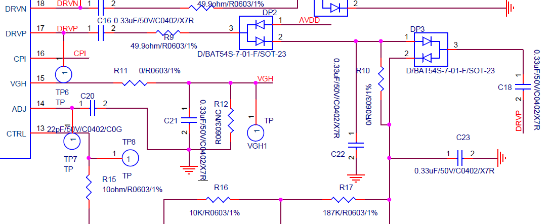
2.Product 20pcs TPS65150 board, just have 3cs board OK, other board's TPS65150 no output voltage. Normal: Vin=3.3V ,Vboost=13V,VGL=-7V,VGH=24V. Fault:Vin=3.3V ,Vboost=3.3V,VGL=0V,VGH=0V.
I test the start-up waveform, find that Vboost and VGL was successful start up and voltage waveform was normal at the begining, but then when VGH want to start boost, then all output voltage was down, and SW ,DRVR, DRVN no switch. then cycled Vin, phenomenon repeat .so do you think what it was happen ?
I think it maybe caused by wrong circuit in the VGH part, I think when resistor R10=0 ohm was connected, C18 should not be connected. otherwise, C18 connected,R10 no connected.
so I removed the C18 ,the TPS65150 work normally,all output and waveform was right. but I am not very well undersanding theory, Could you explain why VGH cann't establish when R10 and C18 all existed ?
Thanks