This thread has been locked.

If you have a related question, please click the "Ask a related question" button in the top right corner. The newly created question will be automatically linked to this question.

UCC28950: UCC28950 constant current output updated schematic check

Part Number: UCC28950
Other Parts Discussed in Thread: PMP8740

Dear colleague,

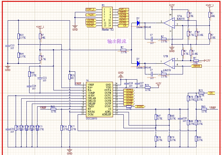
The customer had updated schematic, as below:

Last E2E link:e2e.ti.com/.../778209

The technical requirement of the project customer is working on with UCC28950 is current limiting output.

That is, constant current output after the output exceeds 25A.

Now they have built a schematic of the circuit, and the idea is to use the current signal, compare it with the reference voltage, and adjust the COMP terminal. Please check whether this is feasible. The circuit diagram is as below, and the parameters are not determined.

Thanks a lot!

B.R

Rock Su

  • Hello Rock

    This schematic is closer to what is needed but there are still a few small points that should be changed.

    1/  The on-board error amplifier of the UCC28950 should be configured as a voltage follower. EA- connected to COMP and the output of the external error amplifiers connected to EA+. This arrangement is shown in the document at The usual way to implement a CI/CV characteristic is to use two external error amplifiers and to configure the on-board error amplifier of the UCC28950 as a voltage follower. This is described in the attached note. /cfs-file/__key/communityserver-discussions-components-files/196/CI_5F00_CV-Characteristic.docx

    2/  When the on-board error amplifier is configured as a voltage follower there is no need for any compensation components around it. The loop compensation is provided by the external error amplifiers U7A and U7B in the customer schematic.

    3/ The external error amplifiers should be configured with a type 2 compensation network.

    4/ The schematic is not very clear but it seems that U7A is using GND as a reference through R7 (?). U7B is using a voltage derived from a +12V rail. Both of these error amplifiers require a stable reference and the best source for this is the VREF pin of the UCC28950. Potential dividers from VREF can be used to generate a stable reference - possibly the same reference could be used but that depends on the scaling decisions made by the designer. Again, the schematics in the links below will show a general approach. The designer will also have to decide if the VREF pin voltage is accurate enough to meet their specification.

    5/ Schottky diodes are probably a better choice for the oring diodes at the output of the two external error amplifiers. The PMP8740 design used BAT42WS-7-F parts for example - but in reality most small signal Schottky diodes would be suitable.

    The general arrangement is shown in our PMP8740 reference design - there is a full review of this design at https://www.ti.com/seclit/ml/slup348/slup348.pdf and  https://www.ti.com/seclit/ml/slup349/slup349.pdf

  • Many thanks for your powerful support!

    The customer has started layout.

  • Hello Rock

    I'd be happy to review their layout and schematic if they would like me to, you can email files to me at colingillmor@ti.com 

    In the meanwhile, I'll mark this thread 'resolved' and close it.

    Regards

    Colin