This thread has been locked.

If you have a related question, please click the "Ask a related question" button in the top right corner. The newly created question will be automatically linked to this question.

BQ77905: Upper BQ77905 CTRC/CTRD contected to VSS in 13S

Part Number: BQ77905

Dear Colleague,

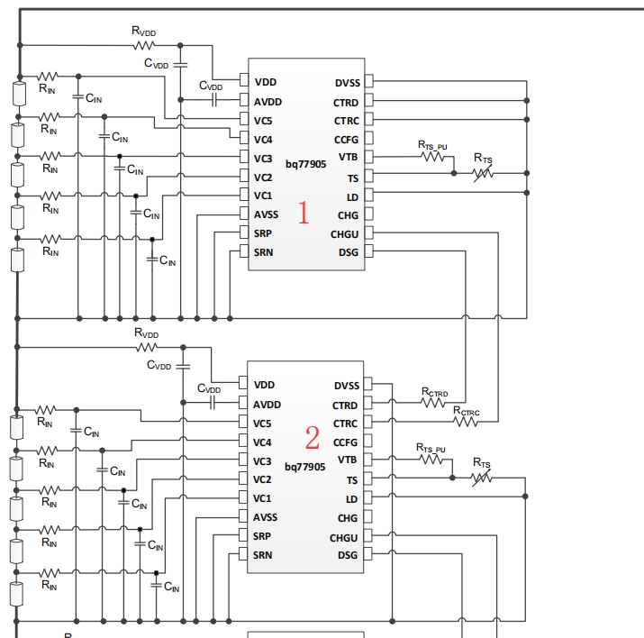
In the case of multi-chip cascade, chip 2 transmits protection action by receiving CHGU/DSG signal of chip 1. Under normal circumstances, the high-level output of CHGU and DSG pins of chip 1 can be detected by the CTRX of chip 2, so chip 2 can be judged that chip 1 has no protective action. However, the CTRD and CTRC of the chip 1 are connected to the ground, which is the same as the signal that the chip 2 receives when the chip 1 is protected (CHGU/DSG is low). In both cases, the inputs are the same, but the output is different.

So how to explain this logic?

Thanks a lot!

B.R

Rock Su

  • Hi Rock,
    The CTRC and CTRD are inputs to the bq77905 to provide external control of the FET outputs in addition to the internally determined conditions. The CTRC and CTRD inputs have 2 voltage regions where they are enabled, see Figure 16 of the data sheet. This lets them be tied to VSS on the upper part (unit 1 above) to allow normal operation, or to the CHGU and DSG from an upper part when used as the lower part in a stack (unit 2 above). The inputs are combined by internal logic for logical control of the outputs, see Figures 15 and 14 of the data sheet.
    To say it in a different way, for unit 1, the external inputs are always OK. For unit 2 the external inputs are only OK if unit 1 is OK.