Hi,
I have replaced the failed switches (TPS22965NQWDSGRQ1 & TPS22965QWDSGRQ1) with the new one.
Both switches are started to work fine after the replacement.
After some period of time, TPS22965NQWDSGRQ1 switches alone failed.
As I mentioned earlier, we are not able to trace the root cause for this also.
The only difference between both the switches is "Quick output discharge". The switch which has this feature is not failing often.
So, please give me a clarification for the following questions :
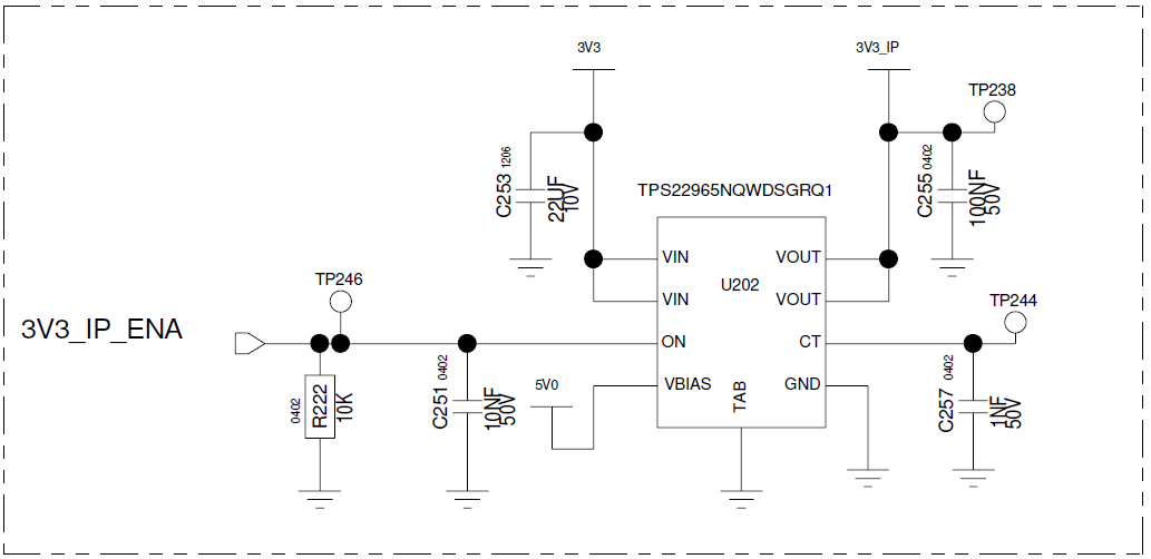
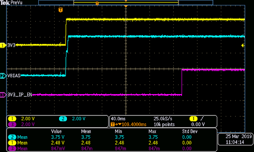
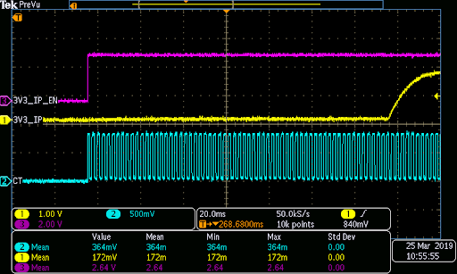
- Is there any timing restrictions are there in the slew rate of VIN and VOUT voltages (power up and power down)?
- Is there any timing restrictions between slew rate of VIN and VOUT with respect to slew rate of CT pin voltage?
- Do you have any diagnostic procedure for the verification of failure of internal MOSFET and switching circuitry?