This thread has been locked.

If you have a related question, please click the "Ask a related question" button in the top right corner. The newly created question will be automatically linked to this question.

BQ24133: BQ24133

Part Number: BQ24133
Other Parts Discussed in Thread: BQ25713

Dear,Sir

I Previously Posted regarding the BQ24133 IC and tested the IC.

After all the bugfixing in the charging section.

We are now getting the output of 1A of the charging Current.

List of issues we are still facing are mentioned Below :

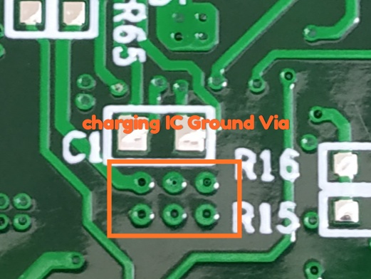
1)IC is rated to deliver the output of 2.5A .But even if we set the charging current to 1A the IC Gets heat up.Please explain the reason and solution for this.

2)I am using 4650 mAH  Battery with PCM. When the battery goes in the full discharge mode,And then we start the charging the charging IC Dosen't provide the supply.I externally provide the excitation voltage of around 15 V to wake the battery to normal form.Is this the issue of the battery or the charging IC.?

3)In our system we are using type c charger and and taking the output of 15 V 3 A.The load we are using is restive type rated at 3A  and 12 V .So due to the increased voltage it consumes more current.Can you suggest me any way so that is can reduce the voltage that will be going to drive the load or reduce the current going in the load. 

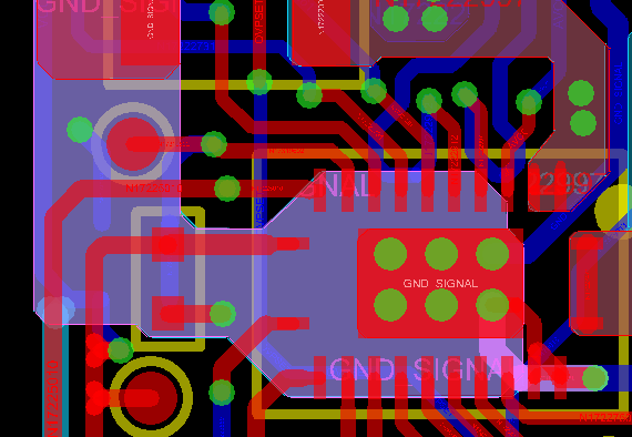
I am attaching you the Schematic.

Please provide some solution.BQ24133 SCHEMATIC.pdf

  • Hi Tirthal,

    Regarding 1, the IC's internal FETs are not lossless. Therefore, the IC's thermal pad must be soldered down to a large ground plane, most likely using vias to either an internal ground or bottom ground plane.

    Regarding 2 and 3, is FB9 populated? If so it is shorting the battery to the load. The battery FET is only comes to connect the battery to the load when there is no input power source.

    Regards,
    Jeff

  • Regarding 1,We already provided the Ground plane in 3 layers,And patch them with the via.So proper grounding is also provided.

    I am attaching you image of the layout.Please see.

    Regarding 2 and 3,FB 6 is DNP component its not placed in the PCB.So no issue for that.

    Also it would be great if you suggest any other charging ic which we can use in our PCB...?

    Waiting for your reply..!!

  • Hi Tirthal,

    Smaller internal ground planes, like the one shown above, don't provide much heat sinking. Is one of the ground layers the bottom layer?

    Have you connected your load and battery to the BQ24133EVM to see if the same heating problem occurs?

    If you only need 12V system from either 15V input or 12.6V fully charged battery, I recommend a 3A buck converter between output of charger and 12V system load. The buck converter would need to have 100% duty cycle so that its output can follow its input when in battery only mode.

    The BQ25713, I2C controlled charger with external FETs, has power path and can therefore provide a minimum system voltage so you might not need the external buck converter but you would need a host and software to configure the I2C resistors.

    Regards,
    Jeff
  • Dear ,Jeff

    We have not kept the ground plane in the bottom layer but we have patch with via.

    Thing i want to share with you is that , in our PCB we have filled the via with the masking.So can this be the heat dissipation issue...?

    I am attaching the PCB Image so please check.

    IC can provide the output of 2 A no issue with that but i worry about the Condition of the IC when i charge with 2A .Because it will get too hot.

    Also i want to confirm that this is the only issue of the heating or any other source affects the IC.

    Yes, we are thinking to keep buck converter after the output of the adapter.

    Regarding the BQ25713 IC We will definitely explore.

  • Tirthal,

    The masking is preventing the IC powerpad from being soldered to the vias. This is likely the problem. I suggest scraping off the mask with a knife and resoldering the IC.

    Regards,
    Jeff
  • Dear,Jeff

    The image that we provided previously was of the bottom side.I am attaching you top view of the PCB.

    Kindly find the image.

    Suggest any solution...!!

  • Tirthal,

    The bottom vias do not appear to be solder to the ground plane for heat sinking. The powerpad must be soldered to a ground plane that is significantly larger than the pad itself for proper heat sinking.

    Regards,
    Jeff