This thread has been locked.

If you have a related question, please click the "Ask a related question" button in the top right corner. The newly created question will be automatically linked to this question.

LM5023: Can't get full load current from flyback converter

Part Number: LM5023
Other Parts Discussed in Thread: UCC28600

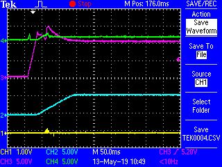
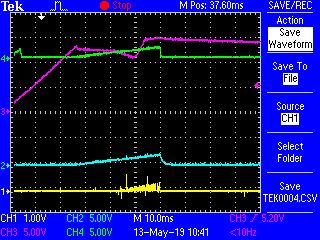
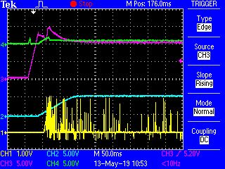
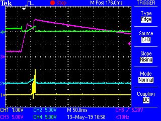
We've designed the flyback converter shown on the attached schematic. It takes 85-265 VAC input and should provide 90VDC at 1A. We cannot seem to get anywhere near full current out of it. The other thing we've noticed is that occasionally, it will not start and remains in hiccup mode. This is especially true when the DC bus capacitor has not completely discharged.SMPS.pdf

  • Hello Don,

    Thank you for your interest in the LM5023 flyback controller.

    From your schematic diagram, I notice 2 main things :
    1. The 68uF bulk capacitor C245 is undersized for a 90W output. For typical flyback designs, the bulk ripple voltage is usually held to ~50Vpk-pk or so. I suggest to double the DC bus capacitance.
    2. The feedback biasing arrangement can lead to poor output voltage regulation. Assuming the D34 shunt regulator is a TL431-like device, it will need a minimum of about 400uA to operate whether the opto-coupler is on or off. Since the feedback current at full power is usually near zero, the opto coupler is turned off which chokes off the bias current for D34. This loses control of full power regulation.
    I suggest to add a 1K resistor across the opto-diode (pins 1-2) to provide a path for 400uA+ bias current when Vf of the opto is 0.4V. This is low enough Vf for the opto to be fully off, but still provide for the minimum shunt current.
    Next, take R204 off of the D36 anode and connect directly to the output cap C242. Increase its value to 368K (using some combination of standard values).

    A few other less critical items:
    3. Consider increasing the value of R203 to 10K to limit the current draw during an output overshoot ( from a 100% step un-load, for instance).
    4. Make sure the D32 (14-V zener) does not clamp the normal voltage that will be reflected from the output to the AUX winding and VCC. It should only be for clamping surges, otherwise there can be high dissipation there.

    I hope this helps you get it working.
    Regards,
    Ulrich
  • Thank you for your response.
    1. I agree that additional bulk capacitance is a good idea however, I see no droop in the DC bus when the load is applied so I don't think this is the immediate problem.
    2. The arrangement you described is exactly the way we originally designed the circuit with the exception of the 1K across the opto. The problem is that until D34 starts conducting, nearly the entire 90V gets applied across it which exceeds it's max anode to cathode voltage. That's why we added D35/D36.
  • Hello Don,

    Well, since the DC bus voltage is not drooping, there is not much load being applied to it on the primary side.
    Can you please quantify your observations? Your previous comments were: "... can't get anywhere near full current..." and "... when the load is applied". This implies that you do get some output regulation at a very light load level. How much load can be sustained if you gradually increase load to the shutdown point?

    Please provide the input and output test conditions when you describe a particular behavior. Also, waveforms at key nodes under various conditions are very helpful. I suggest to monitor Vout, Vaux, QR, COMP, VCC, CS, and SS (not necessarily all at the same time). Make sure that SS voltage rises and stays out of the way after start-up and is not an external cause of a shutdown (leaky or intermittent cap C246). The block diagram shows that an OVP detection at QR, or VCC undervoltage, or the overload detection timer will pull SS down internally. Follow up on each of these possibilities. The controller acts on what appears at its inputs. Make sure the input signals are scaled properly to the system, and there is no excessive noise present.

    I understand about D35 and D36. I presumed that D34 voltage would be essentially zero until the output rose above 60V. Once the 2 zeners start conducting, the remaining voltage builds up across D34. If you don't require tight regulation of the 90V output, then you can leave it as you have it. But D34 is regulating the voltage at the top of R203, not the output. To augment my suggestion of moving R204 to the output, consider to add a ~120K resistor from the anode of D36 to GND (to replace the path of R204+R205 to keep D35 and D36 biased).

    Regards,
    Ulrich
  • Hi Ulrich,

    We've capture some waveforms during startup. 

    Cap1 - No load; Ch1=CS, Ch2=SS, Ch3=VCC, Ch4=Comp

    Cap2 - 200 ohm load; Ch1=CS, Ch2=SS, Ch3=VCC, Ch4=Comp 

    Cap3 - No Load; Ch1=QR, Ch2=SS, Ch3=VCC, Ch4=Comp 

    Cap4 - 200 ohm load; Ch1=QR, Ch2=SS, Ch3=VCC, Ch4=Comp

    Any thoughts?

  • Hello Don,

    Thank you for the waveforms. While I am pondering these, can you please provide the information that I requested on your design targets (input, output) and test conditions for the waveforms captured?

    Thanks,
    Ulrich
  • The input DC bus is 160VDC. We're looking to get 90VDC @ 1amp out.
  • Hello Don,

    I'm sorry, I found that you already did provide the I/O targets early on. Please do provide input conditions for the waveforms. Also, please provide the transformer inductance and turns ratios.

    Thanks,
    Ulrich
  • Primary inductance = 256uH.
    Secondary inductance = 145uH
    Aux inductance = 3.5uH
    Turns ratios:
    Np:Ns = 1.35:1
    Np:Naux = 10.33:1

    The captures where taken from a cold start. Cap 1&3 had no load and the unit came up normally
    Caps 2&4 had a 200 ohm load connected and did not come up.
  • Hi Don,

    Alright, in all 4 start-ups, the VDD gets very close to 15V before either topping off or shutting off. From the 200mA start-up attempts, COMP is pulled to GND compared to the no-loads, where COMP settles to 1V or something. Based on the turns ratios, I get Na:Ns = ~1: 0.13, so for 90V out, it would be ~11.74 V at the Aux winding.

    The QR input OVP threshold is 3V, and with 5.11K and 18.7K work out to OVP = 14V at the Aux winding.
    Since VDD looks like it's hitting 15V, I surmise that QR is exceeding the 3-V OVP threshold during start-up.

    It may barely make it past this with no-load, but I think the higher load currents set off the OVP shutdown.
    There are 2 influences at start-up: the soft-start rate and the shunt regulator compensation.
    I suggest to increase the SS cap value considerably and see if you can get past the start-up overshoot without tripping OVP. If this is successful and the dynamic transient response of your loop is acceptable, then that should resolve the issue.

    If your loop response is too slow for dynamic load steps, it may also respond sluggishly to output overshoots such as during start-up. Consider changing C254 from a single cap from ADJ to C to a type-II network, and also reduce C253 if it rolls the frequency response back too much.
    Here is a reference on type-II loop compensation: www.ti.com/.../slva662.pdf

    Regards,
    Ulrich
  • We increased the SS cap to 1uF. That has helped a great deal. We can now start up with a load current of 810ma. Above that, it initially starts but immediately shuts down. The other thing we're noticing is that if we try to restart before the DCbus has dropped to near zero (or we manually discharge C245), it will not restart.
  • Hi Don,

    I'm glad that your making some good progress. I suggest that if 1uF on SS helped get to 800mA, another 1uF might get you the full 1A. That may not be the ultimate solution, but it is an easy test to make.

    Aside from that, reducing SS to get the OVP shut downs again might help with the restart issue. Looking at the Functional Block Diagram in the datasheet, we see that the VCC pin thresholds are 12.5V on and 7.5V off, unless an OVP shutdown is latched at the QR input. In that case, VCC must decay below 5V to unlatch the OVP. I think that is what is happening there.

    Since the VSD pin re-enables the start-up FET when VCC drops to 7.5V, it won't allow VCC to reach 5V to reset the OVP latch. Only removing AC power (or DC as the case may be) will allow the bus voltage to drop low enough to let VCC drop to 5V and unlatch.

    To be blunt, if this is undesirable, you have to avoid OVP at all costs, or build a work-around circuit to drag VCC down below 5V (or disable the start-up FET), or change to a different controller that does not latch the OVP. Or just avoid OVP at start-up if you like the latch-off feature for possible abnormal conditions, provided that OVP is guaranteed to never be triggered under all normal operating conditions.

    Regards,
    Ulrich
  • Increasing the SS cap to 2.2uF did not help; still won't start at any load greater than 810ma. Also, starting with no load and then applying a load, causes it to shut down. So perhaps we have to look at the shunt regulator compensation as you suggested. Unfortunately, loop compensation is not one of our strengths. We can certainly do the math but we're unclear about where to set he poles and zeros.

  • Hi Don,

    I'm sorry that increasing the SS cap didn't get you any further.
    I suggest that you verify that you do know what is causing the shutdown, even with the higher SS cap.
    It may be OVP and may be related to the loop compensation, but it really should be verified so that we are fixing the right problem. Check VCC of the LM5023 to make sure it is not running down to the UVLO shutdown level with the longer SS time.

    In any case, I found another reference on loop-comp that maybe more useful than the first one.
    www.ti.com/.../slua671.pdf discusses compensation for the UCC28600 which is similar to the LM5023 (as far as loop control goes). I can't find anything directly concerning the lM5023 itself.
    But the principles and design techniques are the same, so you should be able to apply it.

    You will need a network analyzer to generate the Bode plots to validate and refine your compensation.
    It is kind of unavoidable. Things may look good on paper, but the paper is only as good as the parameters you plug into the equations. If some real-world parameters are not what you think they are, you won't know it until you test the circuit and find it not behaving as you expected.

    Also, please revise your feedback as I suggested: tie R204 directly to the output and increase its value.
    You want to be sure that you are regulating the output not some intermediate node of variable drop from Vout. Please review my previous post(s) on this topic.

    Refer to Figure 4 of the new app-note. They have Dz form a local low-voltage source for biasing the shunt reg. This removes any transient influence to opto current due to output variations. Your arrangement is not quite the same. The D35 and D36 zeners can transmit transient voltage variations through R203 and these superimpose on the current control from the shunt. This can be handled and accounted for, but it complicates things. Using the Fig 4 way simplifies the compensation design by making the "Vz" node a non-varying voltage. All control then responds only to variations down the R1 path.

    Regards,
    Ulrich