This thread has been locked.

If you have a related question, please click the "Ask a related question" button in the top right corner. The newly created question will be automatically linked to this question.

PMP8740

Other Parts Discussed in Thread: PMP8740, TPS560200, CSD18532Q5B, CSD19533Q5A, CSD19532Q5B, UCC28180, UCC28950

Hello Roberto,

How are you

I resumed the testing of battery charger, in that we are facing problem of output voltage regulation after loading. After testing it I come to know that, Output voltage is stable at Vout signal (across C53-C56 capacitor bank) but at connector J8 I got dropped out voltage. So the problem lies in MOSFET bank of Q12, Q17....while fault finding I gave 12V external power supply to VCC_FB, and 3.45V to Pre_charge P2.2 node. I got voltages as below

V_float=8.6V

Pre_chargeP2.2=3.45V

Voltage at Q32A base-Emmiter= 0.6V

Voltage at D19 Anode= 8.15V

because of 8.15V voltage Q33 is not able to Turn ON and hence MOSFET bank.

Is above voltages are correct?

Also which diodes from PMP8740 schematics represents Dsw1 and Dsw2?

Thanks, 

Anjana

  • Hi Anjana,
    I have sent the questions above to Roberto, please give him a day or so to answer.
    Thanks,
    Robert
  • Hi Robert, thanks for forwarding it.

    Hi Anjana,

    The voltage you read on Q32A BE is correct, but the one you have on Vfloat is too low.

    The differential voltage between emitter of Q8 and the common source of FETs should be 12V (which is the voltage on Chold).

    Are you using the Buck converter with TPS560200 I have in my board?

    The charge pump, formed by Dsw1, Dsw2, Csw works if the switch-node of the Buck converter is running, and need some load: typical a couple watts (which is the power consumption of the digital part).

    Please check the switch-node on net SW and let me know (may be you can attach a screenshot f SW node).

    Best regards,

    Roberto

  • Dear Roberto, 

    Good Morning!

    I have used same TPS560200 Buck convertor, and I load +5V output with 75mA (here microcontroller and LCD card are not connected). Above readings are with 75mA load connected. Is this load is enough? or should I increase the load to 2W i.e 2W/5V= 0.4A?

    Thanks,

    Anjana 

  • Dear Anjana,

    As far as I remember, already 75mA of load on 5V should have been enough to have correct switching on SW node.

    Please check out if by increasing the load to 400mA the floating voltage is increasing to 12V.

    Anyway, if the floating (differential on Chold) voltage is already 8.7V, it should be already enough to turn ON all FETs.

    Please let me know what you find out.

    Best regards,

    Roberto

  • Dear Roberto, 

    I have tested the FET bank and its driving circuit by applying external 12V supply to VCC_FB node. below are the readings across different points 

    in this case vout=2V

    Also I took readings across FET bank at no load and with Load condition when system is completely ON (only microcontroller and LCD card are not connected)

    At No load Vout=53.99V ; Voltage on J8= 53.50V

    Q17 Emiter WRT GND_S: 53.50V

    Q17 Collector WRT GND_S: 53.50V

    Q12 Emiter WRT GND_S: 53.50V

    Q12 Collector WRT GND_S: 53.99V

    With 37.5 Ohm load resister connected to charger

    Vout=53.99V ; Voltage on J8= 5.88V

    Q17 Emiter WRT GND_S: 5.96V

    Q17 Collector WRT GND_S: 5.88V

    Q12 Emiter WRT GND_S: 5.96V

    Q12 Collector WRT GND_S: 53.99V

    At this time gate voltage of FETs was= 8.73V 

    Thanks, 

    Anjana

  • Dear Anjana,

    All voltages that you described look correct. Only at light load (75mA on +5V) the voltage on C57 reaches a minimum of 6V.

    By the way, all FETs Q12...Q17...etc should be correctly driven, because these FETs can already conduct > 20A each when Vgs is > 4V.

    I see that with 1.44A load (by applying 37.5 Ohm on output) the voltage on J8 drops, and this is not possible.

    Please replace all FETs at check again. You may want remove all FETs and populate only Q12 and Q17, just to check the functionality, but limit the output current to max 10A. Then, if everything is working fine, populate all remaining FETs.

    Best regards,

    Roberto

  • Ok. I will check the FETs as per your suggestion.

    Thanks a lot.

    Anjana

  • Dear Roberto, 

    Good Morning!

    Just to confirm with you,  I have selected CSD19533Q5A (100V, 100A) MOSFET inplace of CSD18532Q5B MOSFET as my Output voltage is 54V and output current is 37A. is this OK?

    Thanks, 

    Anjana

  • Dear Anjana,

    The MOSFET you selected fits also this application, because it is able to conduct full current already with a Vgs of 5V.

    Thanks,

    Roberto

  • Hi Roberto, 

    Today at the time of testing MOSFET bank, I come to know that, all 10 MOSFETS populated on DC-DC board are short at Drain to source. it shows dead short outside the board when checked on diode range using Multimeter. Then I checked extra MOSFETs which are unused ,the result is the same; dead short. why this is so?

    MOSFETs are ordered from Mouser electronics.

    printing on MOSFET: CSD19533 TI 81E MEN8 E3

    Thanks

    Anjana

  • Hi Anjana,

    Maybe you enabled these MOSFETs when the load on 5V was ~ 0, which means the floating voltage was too small.

    You have to apply a minimum load (in my case microcontroller + LCD display and indication LED) to the 5V Buck output to make it switching properly.

    If the Vgs voltage on each MOSFET is too small (let' say 4V) it enters linear region and the losses become prohibitive, therefore they fail.

    Please be sure that, before enabling these MOSFETs, the floating voltage is > 6V.

    Thanks,

    Roberto

  • Hi Roberto!

    This might be possible reason for failure of mosfets which are populated on board; but why unpopulated (  extra mosfets which are not used and still in packaging) mosfets are also showing drain to source dead short.they shouldn't.

    Anjana

  • hi Roberto!

    can you please tell me how to select PTC resistor RT1 and RT2 for this application?

    Anjana

  • Hi Roberto!

    Today I remove all the MOSFETs from dcdc board and check the output voltage after loading 1.4A current; the result was same as previous 53.99V drops down to 1.7V. Then i bypass both RT1 and RT2 by shorting it, the result is I get expected output voltage on the connector i.e. 53.92 after loading 1.4A.

    This mean problem lying in RT1 and RT2.
    I used same RT1 and RT2 as used in PMP8740. How to select PTC resistor here

    Thanks,
    Anjana
  • Hi Anjana,

    Sorry for the late reply, but last Thursday was holyday in Germany and on Friday I took one day off.

    When all FETs (Q12...Q31) are off, since the body diodes of Q17, Q26, Q28, Q20 and Q31 conduct in the direction power supply --> load, RT2 will be in parallel with these body diodes. Therefore only RT1 is connected in series from VOUT and the load; this PTC is in charge to reduce current in case all capacitors C53...C29 are charged and on output there is a short circuit, or the battery is reverse connected (as explained in my white paper).

    If, instead, you connect the battery and all capacitors C53...C29 are discharged, RT2 will limit the inrush current.

    That means, RT1 and RT2 are there for protection only: if the current flows through them continuously, after few seconds they will show high Ohm value because they heat up, and protect the load and the power stage.

    BUT these PTCs are needed only for inrush and reverse current limitation, while during normal operation they should be shorted by means of all FETs Q12...Q31.

    If you see that some FETs are already shorted in the original bag, it might be an ESD problem. Before measuring the resistance source-drain, please add in parallel to gate and source a 10 KOhm resistor, in case, by touching the gate by accident, you may had unwanted voltage on gate, which turns on the FET.

    Please let me know if you have questions.

    Regards,

    Roberto

  • Dear Roberto, 

    Sorry for disturbing you in your vacations!

    I got your answer. That mean all mosfets must be ON before loading. In our case I got most of the output voltage dropped in RT1 i.e. 48V that mean Q12, Q25, Q27, Q29, Q30 are not turned ON that time and all the current is passing through RT1.  Only Q17, Q26, Q28, Q20, Q31 are turned ON , as no drop across RT2 correct?  How do you select gate drive components. please help.

    between the time I remove all the FETs and bypass both the PTCs, I got stable output (53.96) at 5A load.


    Anjana

  • Dear Anjana,

    No need to sorry :-)

    You are right: the sequence is:

    1) Connect (or enable) the 400V on J7
    2) Apply 12V on VCC_FB net and have a minimum load on 5V

    3) Connect the battery on J8 or a load

    4) In case you connect a battery on J8, wait at least 5 times the charging constant, defined by RT2 and the total Cout capacitance (here 6 * 470 uF = 2820 uF), therefore RT2 * Cout = 22 Ohm * 2.82 mF = 62 milliseconds; so, 5 times this constant makes 5 * 62 msec = 310 msec.

    5) Enable all FETs (Q12...Q31) by applying 3.3V on net "Pre-Charge P2.2"

    6) Enable the full bridge DC/DC converter, by applying 3.3V on net "ENA_FB P4.7"

    All FETs Q12...Q31 must be ON before you enable the DC/DC converter. If that is not done, then the entire Vout is applied to RT1 and, as soon as it heats up, the PTC switches to high-Ohm state and the voltage on Vout drops (or just the current, if you have a battery on J8).

    Best regards,

    Roberto

  • Hi Roberto, 

    As i need 940uF capacitance at output, so my charging constant will be (22Ohm * 0.940mF)=20.68msec and 5*20.68=103.4mSec. Correct?is this constant used in software?

    Anjana

  • Hi Anjana,

    Your calculation is correct.

    I think I used 200msec in my software, but this time is not critical; just use extra margin and consider increasing this time also to 200msec in your case.

    Thanks,

    Roberto

  • Hi Roberto, 

    My problem is still there. 

    I have check the system by applying microcontroller signal as per the sequence (inrush relay ON, PFC ON, precharge , DCDC On) but still output voltage is dropped. what should i do? I have checked the power stage by bypassing MOSFET bank and PTC and the power stage is working good with load i.e. no voltage drop seen on J8 output connector, but as soon as MOSFET bank and PTC get in circuit, voltage on J8 output connector starts drop on loading. 

    Thanks, 

    Anjana

  • Hi Anjana,

    This is really strange.

    Have you checked that, when you activate all series-FETs by applying 3.3V on the digital line "Pre-Charge P2.2", you have a voltage on R52 (which is the Vgs voltage on each FET) that is > 6V?

    If this is not happening, all FETs may be damaged again. Please double check it.

    Best regards,

    Roberto

  • Hello Roberto, 

    I have checked all the voltages again, there is few mV across R52 resistor when precharge pulse is given. this means MOSFETs are damaged again. why this is happening? should i change MOSFET? there are two available CSD19533Q5A which i am using and other is CSD19532Q5B. which one is better?

    Anjana

  • Hello Anjana,

    If the MOSFETs are damaged, please replace them with CSD19532Q5B, which will involve less losses.

    When  you test again the board, after replacing the FETs, please check that, before enabling these FETs, there is enough differential voltage over C57 / D18.

    If this voltage is > 6V, then enable the DC/DC stage, do not apply any load to J8 and enable "Pre-Charge P2.2". At this point, please check that the voltage on gate-source of all FETs is enough to have them perfectly driven.

    In fact, if this voltage is too low (according to the gate-source threshold voltage of those FETs, Vgs), they enter linear region and get damaged very quickly.

    Now, if Vgs > 6V, then you may apply the load on J8.

    Best regards,

    Roberto

  • Hello Roberto,

    I have tested the system by bypassing MOSFET bank and two PTCs. and good thing is I am able to load 32A to the system.

    today I applied 20A load and after 5mins D7 diode broke into two parts. I used UF5408 leaded diode there as SMD package of MURS360 is not available. What will be the reason of failure of D7? D10 is shows OK. also I used 10uH sheem inductance at T7.

    Thanks,

    Anjana 

  • Hello Anjana,

    As far as I remember, there is some loss on D7 diode (less on D10).

    The diode you are using is PTH and has similar characteristics to MURS360, but due to the package, has worse thermal performance, so I expect with same loss a higher temperature.

    If you replace it with the same part (UF5408) , please check its temperature when you increase load. If it is too hot, please use a SMD diode (best if in SMC package).

    Best regards,

    Roberto

  • Dear Roberto, 

    After looking at datasheets of both diodes I also concluded the same thing. 

    thanks a lot for your timely support dear.

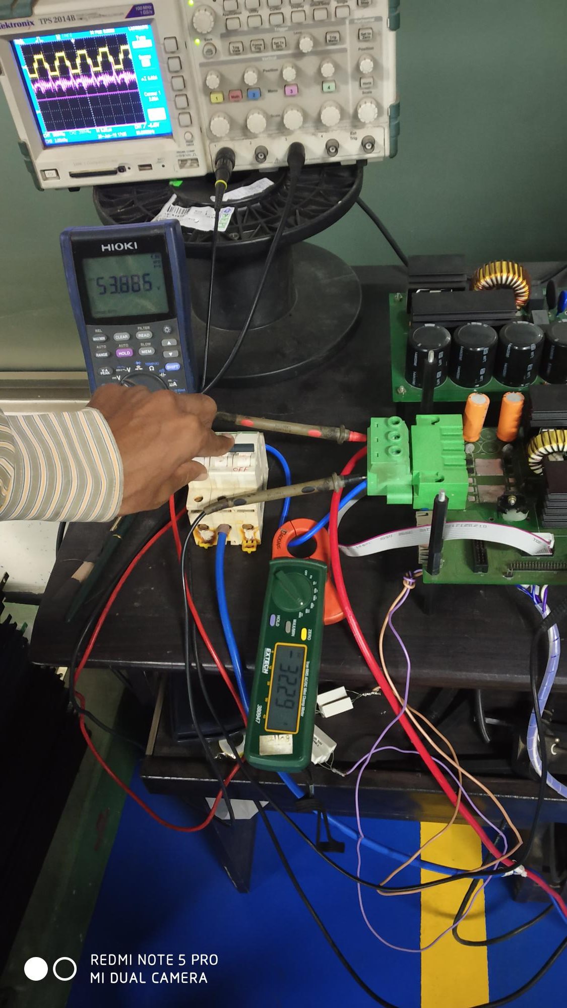
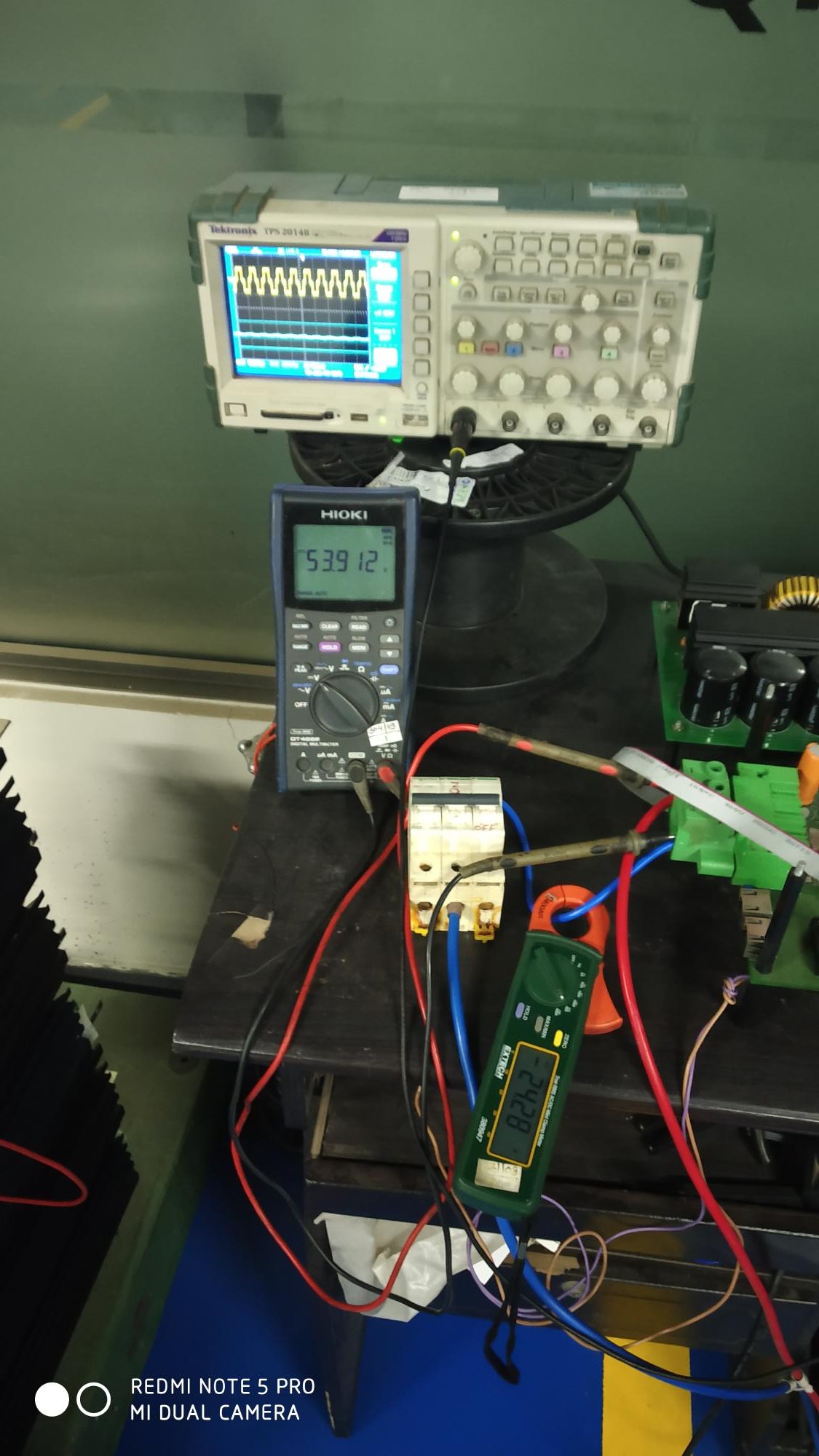
    We have successfully loaded the system with 32A by bypassing Output FET stack and PTCs and get 53.88V at output with 0.943 power factor. 

    yesterday I received MOSFET CD19532. now my next plan is to test by including FETs and PTCs.

    Thanks, 

    Anjana

  • Dear Anjana,

    OK, thanks for the feedback.

    Please check that, when replacing the diodes D7 and D10, you provide enough cooling area for them.

    If you used the same board layout I employed, then you should have no issues.

    Best regards,

    Roberto

  • Dear Roberto, 

    Can you share how to calculate maximum temperature reached in D7, D10 diode and heatsink for them.

    thanks,,

    Anjana

  • Dear Anjana,


    Actually I didn't calculate the conduction and switching losses on D7 and D10 at that time, so I don't have formulas for that.

    You may want to have a look to the following article on IEEE journal:

    "Zero-Voltage-Switching PWM Full-Bridge Converter Employing Auxiliary Transformer to Reset the Clamping Diode Current"

    Though it's pretty complex, therefore I suggest to make a SPICE simulation to check what is the peak and RMS currents flowing through these diodes.

    Best regards,

    Roberto 

  • Dear Roberto, 

    Can I use IXFP72N30X3 mosfet inplace of IPP120N20NFD mosfet with same gate driver? please suggest because my output voltage can be vary from 54V to 60V. and output current is max 37V. 

    Please help.

    Thanks, 

    Anjana

  • Dear Anjana,

    The MOSFET you selected looks OK; just put enough of them in parallel to get reasonable losses.

    Please check out that this MOSFET needs at least Vgs = 7V to be fully driven, so you have to be sure that the voltage on floating supply is sufficient in all conditions.

    Best regards,

    Roberto

  • Hello Roberto, 

    Just for my information.

    After successfully loading with 32A current , we were planned to take detailed readings in last week, at that time we found that AC (Line) voltage waveform was disturbed with spikes on it. and power factor was also degraded to 0.8 . it was because of some other testing going on in our shopfloor. So we load 20A and after two mins , 15A fuse, Rectifier , Current Sense resistors, Mosfets from PFC board and MOSFETs, freewheeling diode, Synchronus MOSFETs from DCDC board get damaged. 

    I wonder is this happened because of disturbed line?

    And why I get degraded PF even though I used PFC there?

    Thanks, 

    anjana

  • Hello Anjana,

    If there is risk of high voltage (and current) spikes, coming from AC line voltage source, I suggest to add a 1N4148 diode, as shown on figure 26 of UCC28180 datasheet. This avoids that during input inrush, a too high negative voltage is applied to ISENSE pin.

    By the way, if there is a damage on PFC, typically this is not involve damage on DC/DC.

    If, on the opposite side, the DC/DC goes into short circuit, then also the fuse, the bridge, the SiC diode will be damaged (and maybe also the Boost FET).

    When you repair it, can you please send over an screenshot of input voltage and current of the Boost stage?

    Thanks,
    Roberto

  • Ok. I will check and let you know. 

    Also , please tell me what is the use of J6 on PFC card? 

    Anjana

  • Hello Anjana,

    If you put a jumper on J6, a small current from Vcc (12V) to VSENSE pin will be added from the part coming from Vout through R9,10,11.

    This way Vout should reach and be stable to ~ 320V. The reason of that is: if there is a problem in the layout (involving high spikes on switch-node) or something goes wrong, you have still margin on voltage on FETs, diode D2 and output electrolytic capacitors.

    Then, if everything works fine, just remove this jumper.

    Best regards,

    Roberto

  • Hi Roberto!

    How can I check gate pulses on PFC board without connecting L1 and D1?

    Thanks,

    Anjana

  • Hi Anjana,

    Another purpose of the jumper J6 is to disable the open loop protection of the PFC; by shorting J6 you apply 1.38V on VSENSE pin, therefore enabling it.

    This way you should have pulses on the gate driver (with high duty cycle).

    Best regards,

    Roberto

  • Hi Roberto, 

    Thanks. I think so that's why I asked you. 

    Also

    I am using iron powder core KT80-26 from KDM. datasheet is attached. as per my calculation I need 10uH inductance for sheem inductor. My calculation is correct ? and is it ok that for 100KHz frequency selected core is suitable? or I should go with ferrite core?

    Anjana

  • Hi Anjana,

    I see that the -26 powder is suitable for filtering or for low frequency (<50KHz). It is not suitable for resonant converters (and this zero voltage switching DC/DC converter needs a shim inductor that can be assimilated to a resonant one, because of the peak-peak ripple current).

    For this reason, I suggest to use ferrite core, for example N87 or N97 from EPCOS.

    Best regards,

    Roberto

  • Thanks Roberto,

    Can you provide me details of core and wire of resonant inductor you used in pmp8740?

    Also for output inductor and pfc choke i should use ferrite core?

    Thanks

    Anjana

  • Hello Anjana,

    The details of core and bobbin are described in the 2017-2018 presentation file of PSDS Seminars (you can download the whole documentation on our WEB site).

    I attached the slide where this information is described (slide 26).

    Therefore, to summarize, the bobbin is a PQ20/20, with N97 EPCOS core, with a gap of 0.77mm.

    Delta-B is 118mT, while ue = 57.

    Here I wound 10 turns of LITZ wire (160x0.1mm).

    The copper loss is 0.63W ad core loss 0.57W.

    Regarding PFC, you can use a toroidal choke from Kaschke, SDR18 with part number 170.806, or, like I used, wind it by yourself using "Kool-Mu" core or NKL, which are iron powder cores. You cans use the same core for the output inductor.

    Best regards,

    Roberto

    SEM2200 Design Review of a 2kW Parallelable Power Supply Module - Slide 26.pdf

  • Thanks Roberto, 

    Please tell me how do you calculate core loss and copper loss?

    Anjana

  • Hello Anjana,

    Copper loss can be calculate pretty easily with the formula Pcu = Rdc * Irms^2, where Rdc is the DC resistance of the winding, and Irms is the primary side transformer RMS current.

    The resistance Rdc can be calculated according to the datasheet of the bobbin, downloadable under:

    On page 3 of this datasheet it is shown the mean length of one turn. You have here 10 turns of LITZ wire 160x0.1mm.

    Just search on the WEB for the resistance of this wire, per meter.

    Therefore, since ln is 44 mm times 10 turns = 0.44 m. When you find out what is the resistance of a LITZ wire with 160x0.1mm characteristic, you can calculate Rdc. You should know already what is the RMS primary current of your project.

    Core loss:

    Please download the datasheet of N97 material:

    Please go to page 5 and have a look to the relative core losses versus temperature at 100 KHz (which is your switching frequency). Worst case is at 25C, so please consider this temperature.

    At 118mT (which is your deltaB(peak)) the relative loss is ~ Pr = 150 KW/m3.

    Than consider the previous datasheet, and on page 2 you can read the volume of the core-set (Ve) which here is 2843 mm3.

    At this point you multiply Pr * Ve = 150 KW/m3 * 2843 mm3 * 10^(-9) (because we are multiplying m3 and mm3) = Pcore. This results into Pcore = 0.426 W.

    This value is very close to what I calculated in the slide I sent you.

    Probably the slight different depends on the reading of the logarithmic chart, showing the relative loss.

    Best regards,

    Roberto

  • Thanks a lot Roberto. 

    Anjana

  •   Hello Roberto, 

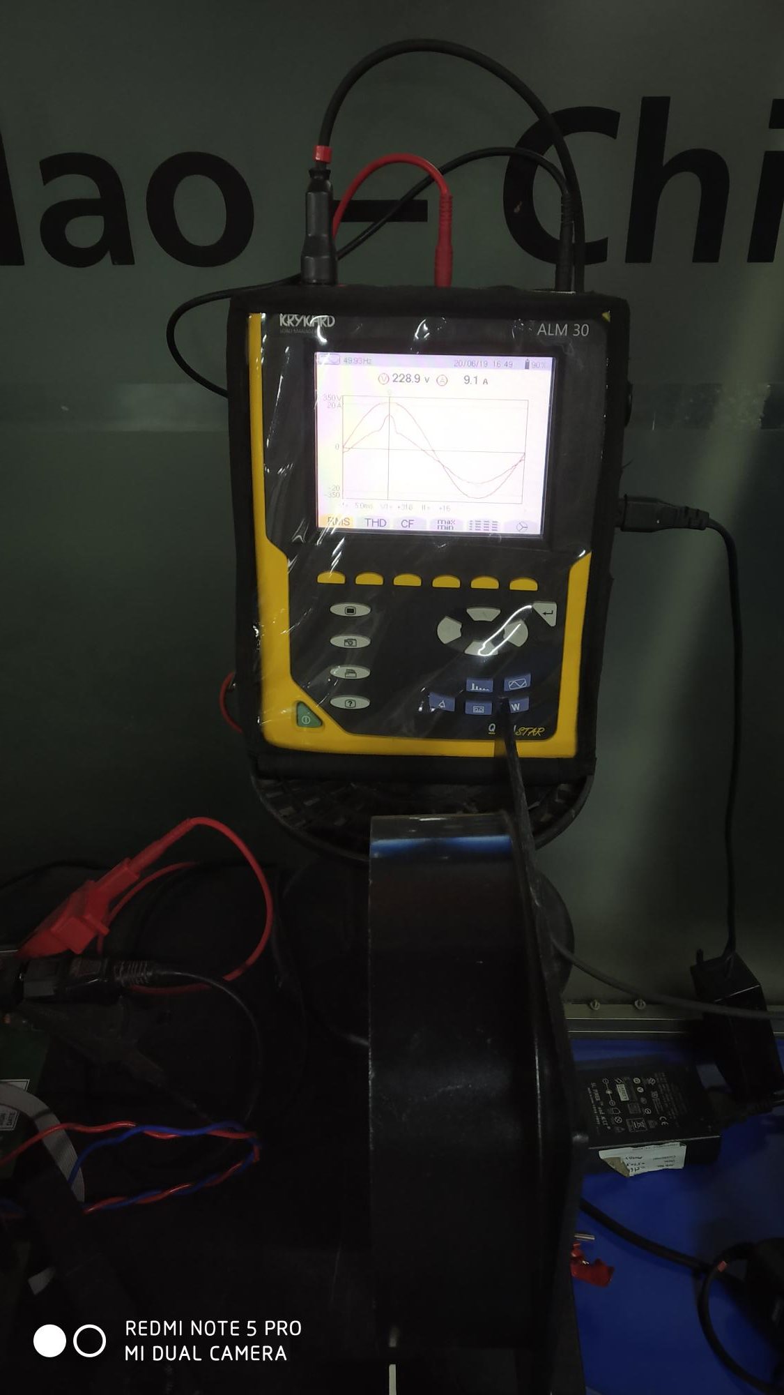
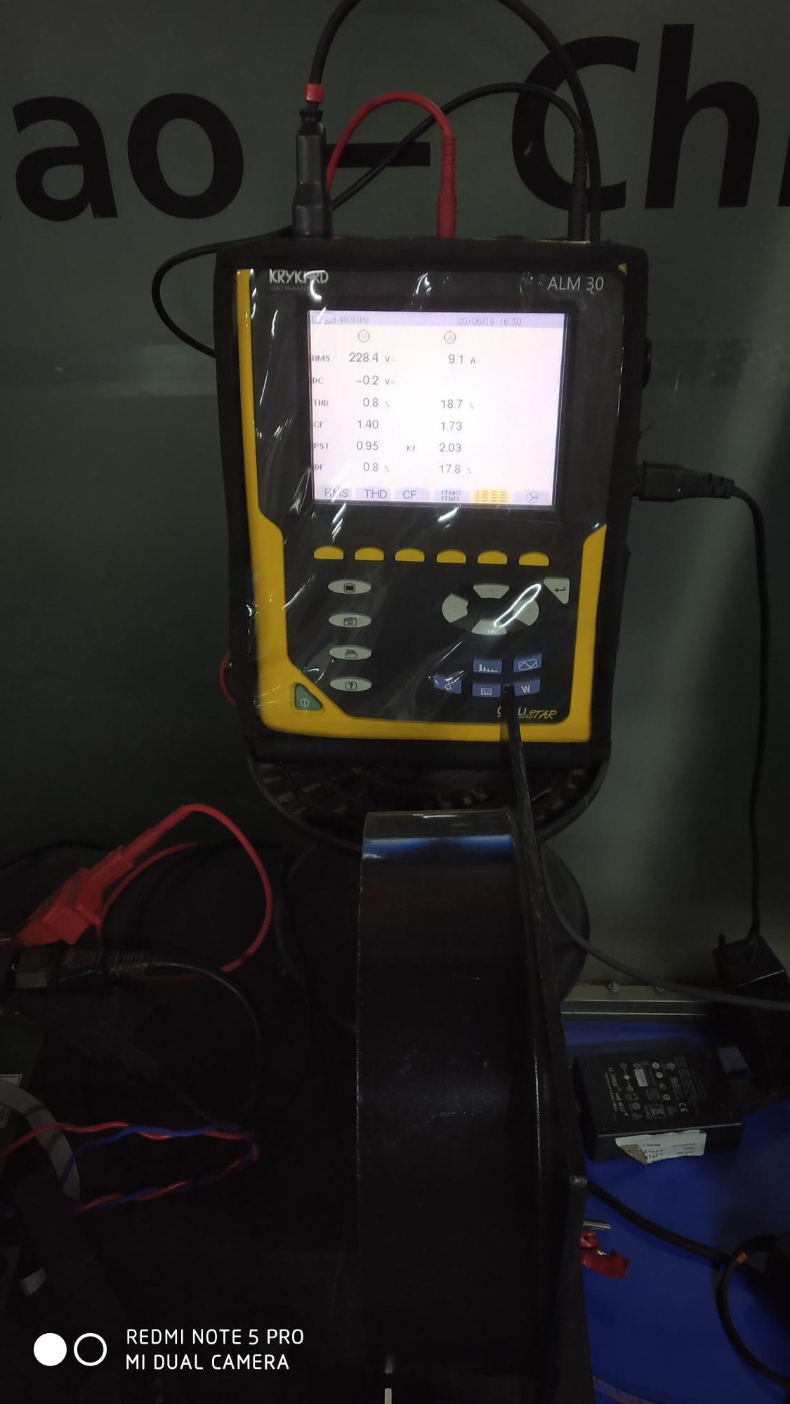
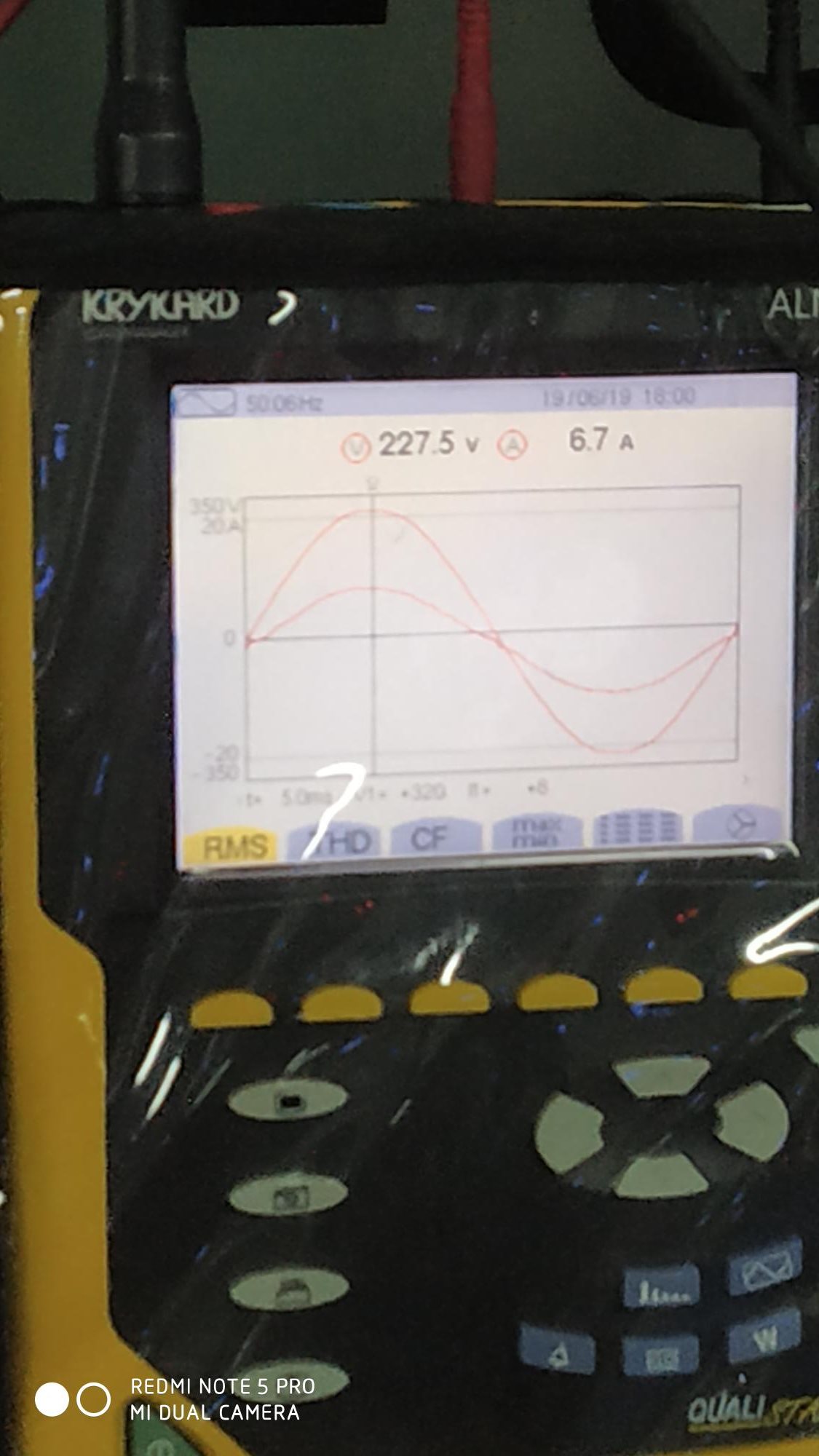
    Herewith attaching some screenshots of testing of system at 32A. these snapshots are before system get damaged. I will share the further waveforms of the system once it get repaired. 

    Also, can you please share datasheet of core used for PFC choke. I am not able to find the same.

    Thanks, 

    Anjana

  • Hello Anjana,

    According to the screenshot of the oscilloscope, it looks like the PFC stage is not working correctly. The spike on top of sinusoidal current should not be there.

    I had the same problem at the beginning, and the reason was that the current sense resistor of PFC stage was too high. Please double check it.

    PFC inductor:

    I made it by hand, by employing two cores in parallel from NKL, part number CM400125 D0522-00. One single core has external diameter = 40mm and thickness 15mm, so when you put two in parallel, the diameter will be the same, but the thickness 30mm.

    I wounded 35 turns of single enameled copper wire, with a diameter of 1.6mm (I added isolation tape before winding; in theory is not necessary, because the core is already coated, but it increases the isolation).

    I tried to download the datasheet of the core I used, but I cannot find it.

    BTW you can have a look to the products from NKL, under the link:

    Best regards,

    Roberto

  • Dear Roberto, 

    1) OK I got it. I have used same 0.03 Ohm resistors 3nos in parallel as you used in PMP8740 ver.C. my requirement of  PFC stage rating is as same as PMP8740 PFC design so, I Used the board as it was.

    2) I am attaching some screenshots of loading at 24A. is this current waveform is ok?

    3)I am trying to check gate pulses on PFC card without populating MOSFETS Q1, Q2, and by putting jumper in J6--->  at 70VAC I got VCC_FB:11.8V, VCC_PFC:15V and at VSENSE pin: 2V  but there is no Gate pulses (I disconnected D1, D2, L1)

    Thanks,

    Anjana  

  • Sorry forgot to attach snapshot of 24A loading

  • Regarding core of PFC choke 

    L=210uH, 

    No of turns : 35T

    hence AL=210000nH/(35X35)= 171.43nH/T2

    you used 2 core hence AL=(171.43nH/T2)/2= 85.715nH/T2 this is required AL value of core. right?

    For this I can see magnetics 55083 core with u=60 and AL=81nH/T2. is it correct? or I should consider AL=171.43nH/T2?

    2) I got attached datasheet. in that part no you mentioned CM400125 is shows AL=168nH/T2 and u=125 also Magnetic's 55254 is looking equivalent for CM400125. Which one I should consider?

     Anjana

  • Hello Anjana,

    You are right: the cores I used have each one 85.7nH/T2, therefore in total is 171.4nH/T2.

    You can use the core from Magnetics that you found: 55083. This way, with two cores in parallel, it will be 162nH/T2.

    When using 36 turns, you get 210uH inductor.

    Regarding the shape of the current you showed with lates screenshots, I see it's perfect!.

    Thanks,

    Roberto