This thread has been locked.

If you have a related question, please click the "Ask a related question" button in the top right corner. The newly created question will be automatically linked to this question.

UCC27714: Outputs of driver latching in state despite input changes

Part Number: UCC27714

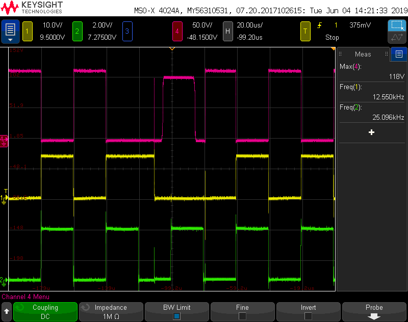
I am using two drivers to control either side of an H-bridge. One if these drivers has an issue where the outputs occasionally latch and hold their state such that they do not match their corresponding HI/LI input. [See attached image: Green - LI, Yellow - LO, Pink - HO.]

The main recurring issue is when the LI input transitions to low but the LO output remains high. The HI input is the inverse of LI and also does not change at this point. Some amount of time after the input change (>1us), the output changes but then misses the next edge and so on. This continues for several cycles before the driver catches up again.

The PWM drive signal is running at 25-26kHz with 50ns deadtime between LI and HI inputs. I have tried: replacing all hardware, adding capacitors to the LI/HI inputs, increasing the capacitance of the supply capacitor.

From the datasheet I cannot see any situation whereby the LO output would be high whilst the LI input is low. Can anyone explain why this may occur?

The supply rail does not drop out, nor is there any issue with the inputs to the driver.

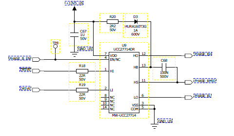
See schematic below:

  • Hello Matt,

    Thank you for the interest in the UCC27714 half bridge driver. I am an AE with the High Power Drivers group and will work to address your concerns.

    I assume you have some small filter capacitance on the driver inputs based on your comments. Confirm the capacitors are close to the driver HI/LI pins and VSS pin with short length trace connections.

    The UCC27714 datasheet has some sections that describe conditions that may result in the driver output not being in the correct state. See the datasheet here: http://www.ti.com/lit/ds/symlink/ucc27714.pdf

    Section 7.4.5 describes operation with negative voltage on the HS pin with respect to COM. If the HS pin negative voltage exceeds the datasheet rating, the HO output can be in the incorrect state.

    Section 8.2.2.5 describes driver output operation if the HS dV/dt rating of 50V/ns is exceeded. The dV/dt can be reduced by increasing the gate resistance value.

    Section 8.2.2.0 describes driver output concerns if the LO or HO output overshoot or undershoot exceeds the datasheet ratings. Increasing the gate resistance can help reduce overshoot/undershoot on LO or HO. Also placement of schottky diodes very close to the driver pins LO and COM or HO and HS for undershoot and LO and VDD or HO and HB for overshoot clamping. Use 1A rated parts in small SMT packages for ease of placement, and low Vf.

    Please confirm if this addresses your concerns, or you can ask additional question on this thread.

    Regards

    Richard Herring

  • Hi Richard,

    I have read through the datasheet and your comments but cannot find anything to explain what I am seeing. The odd behaviour is that the LO side is erratic, not just the HO. HO is more commonly unresponsive due to the reasons you listed, but there are no documented case where LO would be high when LI is low - see image. Most documented failure states force the outputs low regardless of input state. There is nothing to suggest that the output states would be stuck high regardless of input state (potentially dangerous).

    It seems to be that the device fails to respond to the edges of both inputs and takes several microseconds to catch up. Are there any known cases where a device will be locked in its current state - regardless of input transitons - particularly when the inputs are low but the outputs are high?

    From experimentation - this behaviour seems to occur when there are high currents flowing through the controlled H-bridge (>1A). Input PWM deadtime seems to have an effect: a larger deadtime reduces the frequency of these errors.

    Thanks,

    Matt

  • Hello Matt,

    We have had feedback in some applications where the LO and/or HO can exhibit the incorrect state based on the driver inputs.

    The incorrect state of the driver outputs is normally related when there is excessive overshoot or undershoot of the driver output. Adding the Schottky diodes from the driver output, very close to the driver pins from HO/LO to HB/VDD and HS/COM can resolve these issues.

    The HO missing pulse or short HO pulse is usually related to HS dV/dt over the 50ns datasheet limit. Increasing the gate resistance can help reduce the HS dV/dt slew rate.

    The statement you made regarding increasing the deadtime may indicate there is a dV/dt concern, as the increased dead time would allow the IC recovery time from the transient event.

    Please confirm if this addresses your concerns, or you can post additional question on this thread.

    Regards,