This thread has been locked.

If you have a related question, please click the "Ask a related question" button in the top right corner. The newly created question will be automatically linked to this question.

BQ24610: BQ24610: Migration from BQ24610 to Bq24630 bis

Part Number: BQ24610

hi,

sorry for the delay, I was waiting for more feedback.

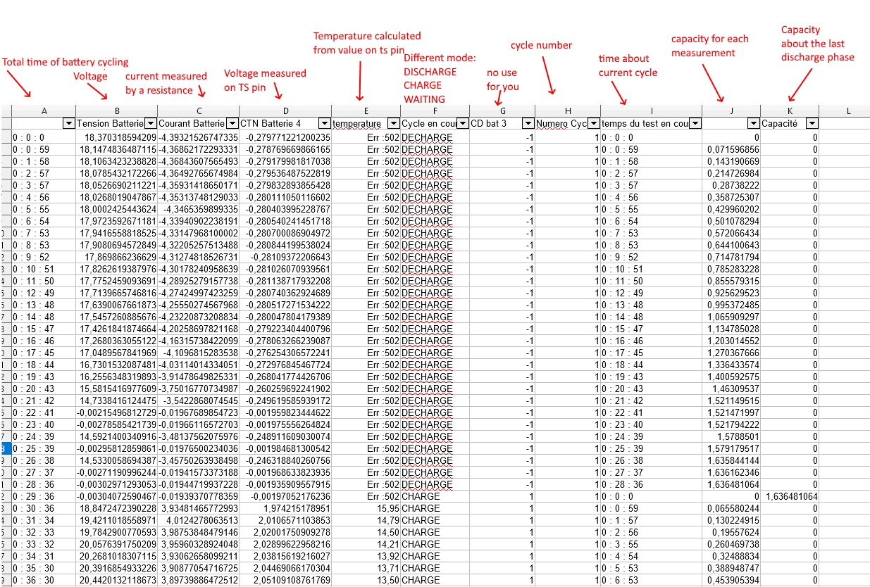
I attach an excel file about my battery cycle. please follow the link (size 23MO)  https://transfernow.net/10kfn2o18q7u

battery specification : 21V 5A/h

current load : 4A

you can see on it fluctuation of the charging time. I don't know what's append and I would like an issue.

sometime end of charge after 30 min, other more.

I have another PCBA with the same design and component without any problem.

if you have more question, don't hesitate to contact me.

Kind regards

raphael MARC

  • Hi Raphael,

       I am not allowed to open external links. Can you attach the actual excel file with the results here?

  • Hi kedar,

    my file is higher than 20 mO so I can't post on it.

    I send to you 1031 cyclesResult_batt4_partie1.xlsx

    thanks,

    Regards,

    Raphael MARC

  • Hi Raphael,

       What is the difference between Tension, Courant and CTN Batteries, what is the column between time of test and capacity, and what does attente refer to in the charge cycle column? Also was there any change in schematic or layout between the working board and non-working board?

  • Hi Kedar,

    except the IC component BQ24 and resistors for the VFB, there is not change on schematic and layout.

    normally, we have a battery pack with a capacity of 5Ah.

    I explain column as below:

    thanks

    Regards

  • Hi,

    any update about my problem?

    thanks in advance

    kind regards

    Raphael MARC

  • Hi Raphael,

       You mentioned your battery voltage is 21V, and looking at the graph that is around the voltage the Cycle en cours column changes from Charge to Attente which is when charging stops. What is the resistor divider values for VFB that you use to set charge regulation voltage? From the looks of it, it looks like current is tapering down in the constant voltage phase of charging as battery nears fully charged signifying the end of the charge cycle.

  • Hi Raphael,

       Plotting your battery voltage and charge current across time in excel (similar to Figure 13. Typical Charging Profile) will give you more information than analyzing the raw excel files. Let me know if this resolved your issue or if there are further questions.

  • Hi Kedar,

    OK I change excel files to give you more information.

    to reply at your last post, Attente means that a dynamic load is not ready for this battery pack.

    currently we proceed at a long battery cycle charge to validated cells life.

    thanks for your time.

  • anyway, how could I send to you schematic?

    I can't post here because it's a confidential information.

    thanks for your reply

  • Hi Raphael,

       I have sent you a friend request through which you can send me information confidentially through private message,

  • Hi kedar,

    thanks, I send to you my schematic and PCB binder.

    perhaps you could find pcb problem for my charging problem.

    kind regards

    Raphael MARC

  • Dear Kendar,

    Have you got an update about my problem?

    thanks in advance

    Kind regards

    Raphael MARC

  • Hi Raphael,

       Looking at the schematic, it looks good. You mention 3.7A but I calculate fast charge setting of 2.517A. For layout I would recommend you keep your C12 (VCC cap) and Q8(HSFET) Q9((LSFET) loop tight as possible. This allows you to bring in your BTST cap (C21) closer as well.The resistors for the resistor divider at ISET1/2 and ACEST are not important to be close to the IC and can be further away. Even C14 C15 (output capacitors) should be closer to the IC, as increased impedance and the possibility of other portions of the circuit coupling on the trace back VFB could be problematic. The above 2 are more critical for chargers. Have you been able to show your charge cycle as a full charge profile? This will be very helpful for me to see what stage of the charging that might be failing so I can isolate the issue.

  • Charge profile similar to Figure 13. of BQ24610 datasheet.

  • Dear Kedar,

    thanks for your investiguation.

    I saw on an application note (SLUA585) figure 8, that IC need a capacitor (C5) between drain of top mosfet to source of bottom mosfet.

    what is the effect of this capacitor?

    I see also on my schematic than we don't differenced PGND and AGND.

    that could be increase noise signal. i'm right?

  • Hi Raphael,

       Let me slightly amend my above statement. C12 (VCC capacitor) is your VCC decoupling capacitor and all decoupling capacitors should be placed as close as possible to the IC. The high frequency loop whose are you want to minimize would be your input capacitor, Q8, Q9 loop. The C5 mentioned in the above application note is the input capacitor to the high frequency loop. Connecting it across the drain of high side mosfet, and source of low side mosfet will help make that loop tight, and reduce ringing and EMI. For your schematic you have C8 so make sure C8, Q8, Q9 are connected in a tight loop close together. 

      Yes, separating PGND and AGND is important, especially for your application's charging current. This way your PGND can be your high current carrying ground, AGND can be your small current carrying ground, and this helps  to avoid small signal ground coupling high current (high di/dt) ground noise, which can cause slight ground shifts. Have a separated PGND and AGND, and join them together with a net-tie under the IC.

  • dear kedar,

    on my PCB layout, C8 is far away of IC. so I need put a new one close to Q8and Q9. when I put it my noise signal is lower.

    I try a full charge today and give a result this afternoon or tomorrow.

    I'm on holiday next week and during 3 weeks so after I couldn't do something before the 18th of august.

    kind regards,

    Raphael MARC

  • Hi Raphael,

       See E2E direct message as well. 

  • Hi Raphael,

       Closing thread for now. Feel free to re-open the thread when you are back and able to get the information.

  • dear KEDAR,

    after put a capacitor between drain and sources of the power charge system, my charge could finish properly.

    I try a new cycle charge and I give to you the result.

    thanks for your patience and your technical support.