This thread has been locked.

If you have a related question, please click the "Ask a related question" button in the top right corner. The newly created question will be automatically linked to this question.

TPS92691: Unexpected waveforms and not working properly

Part Number: TPS92691

Hi, I'm working on an LED driver board, and I'm running in to some unexpected behaviors.    (Please see attached scope screen shot).

Topology:  Boost.

Vin:  11 volts

LEDs:  a chain of 5 with a forward voltage of 2.8-3.5 volts depending on current

Using low-side LED current sensing, Rsense = 0.10 ohms,  Viadj = .14 volts

Using PWM dimming, with a low-side FET

So, the questions are: 

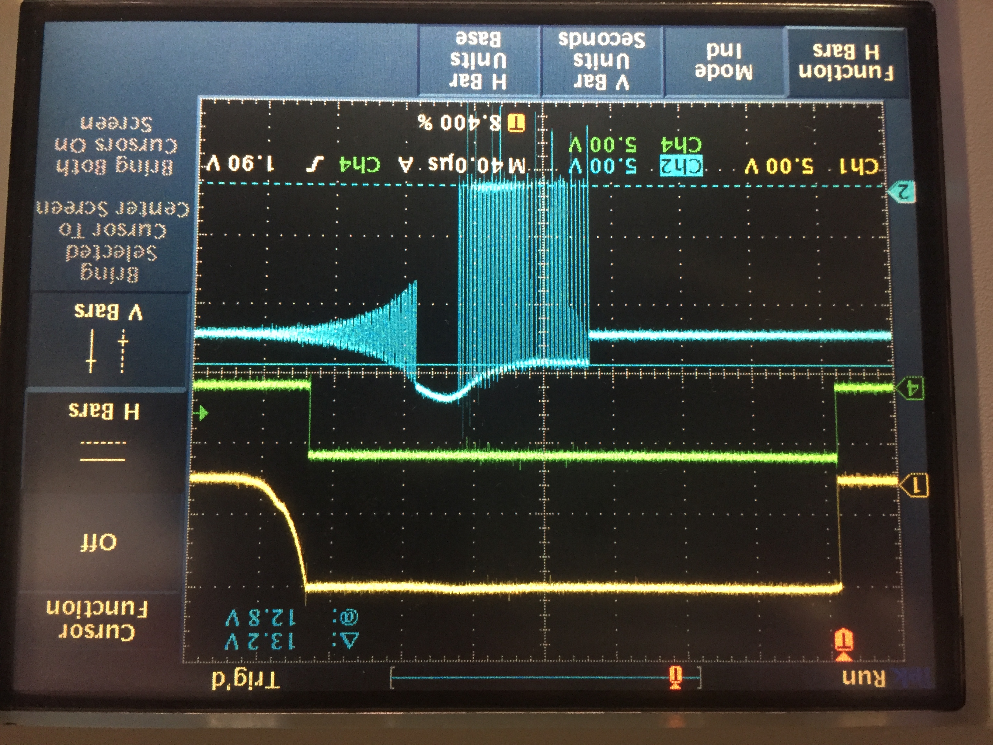
Why is the switching not even starting till half-way through the On-period?

Why is the LED voltage rising?

Why is there some ringing a little bit after the switching shuts off.

And any thoughts or theories as to what could be causing this?

For the screen shot: 

   Channel 1 (yellow):  the PWM FET Gate voltage

   Channel 2 (blue):  the voltage at the Source of the switching FET.

   Channel 4:  The PWM input signal.

Thanks in advance!

-Michael Shonle

  • Hi Michael,

    We did not get the scope capture.  Please attach it and we can comment on it.

    Thanks Tuan

  • Sorry, Hopefully it worked this time, thought I had already done it...

  • Hi Michael,

    First with VIAJ at 0.14V...This is on the really low side of what the part can accept (see section 7.3.7) because of the offset in the current sensing circuit.  How low of a current are you trying to control?  Please give us your specification as far as output voltage range of the LED and the current range.  In addition, please forward me your schematic.  I'll comment more when I get these from you.

    The ringing at the Source of the switch FET that is ringing at the end is to to the current in the inductor discharging when the FET is off and going to zero current.  This is normal for any FET and inductor switching circuit.  The ringing is the natural frequency of the inductor and any parasitic capacitance it has on it.

    Thanks Tuan

  • Hi, and thanks so much for your help! 

    In terms of the overall design, we are actually wanting to run a chain of 15 LEDs at 5 amps pulsed (so about 60 volts total), with a 1 % duty cycle, but wanted to start slow and work our way up.  We did try increasing the Viadj to 0.8 volts, but that was even more erratic, with the voltage to the LED going even higher and then shutting it off at apparently the OVP reaching its threshold of 70 volts.

    Here's the schematic, as a pdf, not sure if it's attaching right.

    IrSuperDriver_A.pdf

  • Hi Michael,

    The instantaneous power level is really high at 300W.  Did you go thru our design calculation to get your values?  From the schematic the values seems wrong.  The inductor value listed is 26uH but the part number is a 68uH.  In actual design it should be closer 6.8uH-12uH based on your switching frequency of 420KHz (Rt=18.2k).  The schematic shows 24V input...What is the minimum input voltage?  You will need that for the calculation.

    You should not use R14 and D01 unless there is some reason for this.  The turn off time will be slow with this...You should start out with like a 0-10 Ohm on R14 to begin with.

    The compensation seems quite high BW.  You should start with R46 as zero Ohm and C61 around 0.1uF-0.22uF just to get the system stabilized first and you can compensate better later with transient response or sweep the loop.  What you are calling 'erratic' is most likely instability of the loop and this will help with that.

    I would start with low current like you are doing (VIADJ = 0.8V) then adjust up as needed.

    Thanks Tuan

  • Hi, and thanks for the followup.   Regarding the Input voltage, this will be tightly regulated so Vin == Vin(min), and we initially designed for 24 volts but we can also change it if needed.

    Yes, we did use the design calculations in the datasheet, maybe you can help clarify in case I mis-understood them.  (and yes, there's an error in the schematic inductor name, it is in fact a 68 uH, which is what the design equations seemed to be computing, based on:)

    V in = 36 volts    V LED = 60 volts,  I led = 5 amps.   Fsw = 420KHz

    Dmax = 0.4

    If we assume a 5% ripple,

    DeltaI = RR * I led / (1 - Dmax) = .05 * 5 / (1-.4) =   .42

    From Equation 8:

       L = (36 * .4)  / (.42 * 420000)  == 81 uH.

    If I use eqn. 11 instead, then it computes:

       L = (36 * 36) / (2 * 300 * 420000) * (1 - 36/60) == 2 uH,

    So not quite clear on if these are being applied right?  It doesn't seem to make sense in Eqn. 8 that a higher Supply Voltage would need a bigger inductor, for example.

    Hope you can clarify about this.

    Also, regarding the need for and value of R14, this is based on the datasheet, excerpted here, as well as the schematic for the Evaluation Board, can you please elaborate on your recommendation?

    8.1.12 PWM Dimming Considerations
    When PWM dimming, the TPS92691/-Q1 requires another MOSFET placed in series with the LED load. This
    MOSFET should have a voltage rating greater than the output voltage, VO, and a current rating at least 10%
    higher than the nominal LED current, ILED.
    It is important to control the slew-rate of the external FET to achieve a damped LED current response to PWM
    rising-edge transitions. For a low-side, N-channel dimming FET, the slew-rate is controlled by placing a resistor
    in series with the GATE pin. The rise and fall times depend on the value of the resistor and the gate-to-source
    capacitance of the MOSFET. The series resistor can be bypassed with a diode for fast rise time and slow fall
    times to achieve 100:1 or higher contrast ratios

    (also, note that initially we are starting out with a string of 5 and running it at around 12 volts, but the design values don't seem to change much)

    We will try changing out the R46 comp resistor, though I would note that it is the value specified in Figure 32 (R19 in that schematic) (section 8.2.1), and calculated by Eqn 65), which is somewhat similar to our design.   Also, do you think it would work with just doing the Integral Compensation and not even having a Proportional term? (e.g. Figure 30 vs Figure 31)  And what value capacitor would you recommend?

    Also, in looking at Section 8.1.9, I don't see an equation for just doing Ccomp for the Boost topology, is it permissible to use Eqn. 37 for Boost mode as well?

    Thanks again for your help, and any other changes that you would recommend?

    -Michael

  • Hi Michael,

    I would start with the integral compensation only first and if you need to have higher BW then have the proportional term.  In general, the LED is really a constant load and does not need really high control loop BW. I would start with the calculated CComp or you might go larger 0.1uF-0.22uF to make sure I have loop stability first to trouble shoot. 

    There is a spread sheet calculator under Software on the following link and you can use that to help calculate your values,

    http://www.ti.com/product/TPS92691/toolssoftware

    The PWM FET...You can use the circuit that you currently have but you might find out that you can reduce the resistance to the gate of the FET.

    Thanks Tuan

  • Hi, thanks so much for your suggestions, we replaced the CComp with a 0.1 uF (the spreadsheet suggested 0.04 uF), and the Inductor with a 6.8 uHenry, and it's pretty much working now!  We're using a 0.025 ohm FET Isense resistor (the spreadsheet is recommending 0.050 ohms).

    We do have one additional 'tweak' question: it's taking about 15 uSec to come up to the final output voltage, and we're wondering if it can do it faster?  And what component(s) should be changed?  would a bigger or smaller inductor help, or is the Ccomp, or the ISense resistor, or is this about as good as it can get? 

    It's being powered with 36 volts, and with a chain of 15 LED's, it's outputting about 55 volts, and running at 5 amps (0.033 ohm CS resistor, and Viadj = 2.25 volts).

    Thanks!

    -Michael

  • Hi Michael,

    Since you have 1% duty cycle for your PWM'ing the droop in the voltage when PWM is off is the reason that it takes that long for the voltage to build back up.  The only way to get this faster is to reduce the discharge and increase the BW of the control loop.  The way to do this is to:

    1.  R6 and R5 by a factor of say 3X.  This will give the same effective OVP but reduce the discharge on the output cap during off time.

    2.  Reduce Comp cap but you can get into stability issue.  The other compensation is the type 2 with a series resistor (lead lag network)

    3.  I do not know if R14 is still 10K or not but reduce this to say 100 Ohm to see if it help.

    In reality, the output current is what you are concern with so you scope capture should show the current on the LED and this is the real matrix.

    What system is this being used for?  The other way is to increase your duty cycle by a small amount to compensate for the narrower current pulse if you can.

    Thanks Tuan

  • Hi, thanks for those suggestions, we'll try them out.

    It's for lighting up a camera so it synchronizes to the camera shutter so we may be able to start it a bit in advance, but overall it's really working well enough, thanks for all your help!

    -Michae