This thread has been locked.

If you have a related question, please click the "Ask a related question" button in the top right corner. The newly created question will be automatically linked to this question.

TPS56121: Problem with TPS56121 and recommended circuit on datasheet

Part Number: TPS56121

Hello,

I have designed a 12V to 8V buck converter using  TPS56121. I used the compensation tool (www.ti.com/.../sluc263) to redesign the feedback loop and for Rbias (R7) I am using a variable resistor to adjust the output voltage. I have used the same design given on datasheet Figure20 page 15.

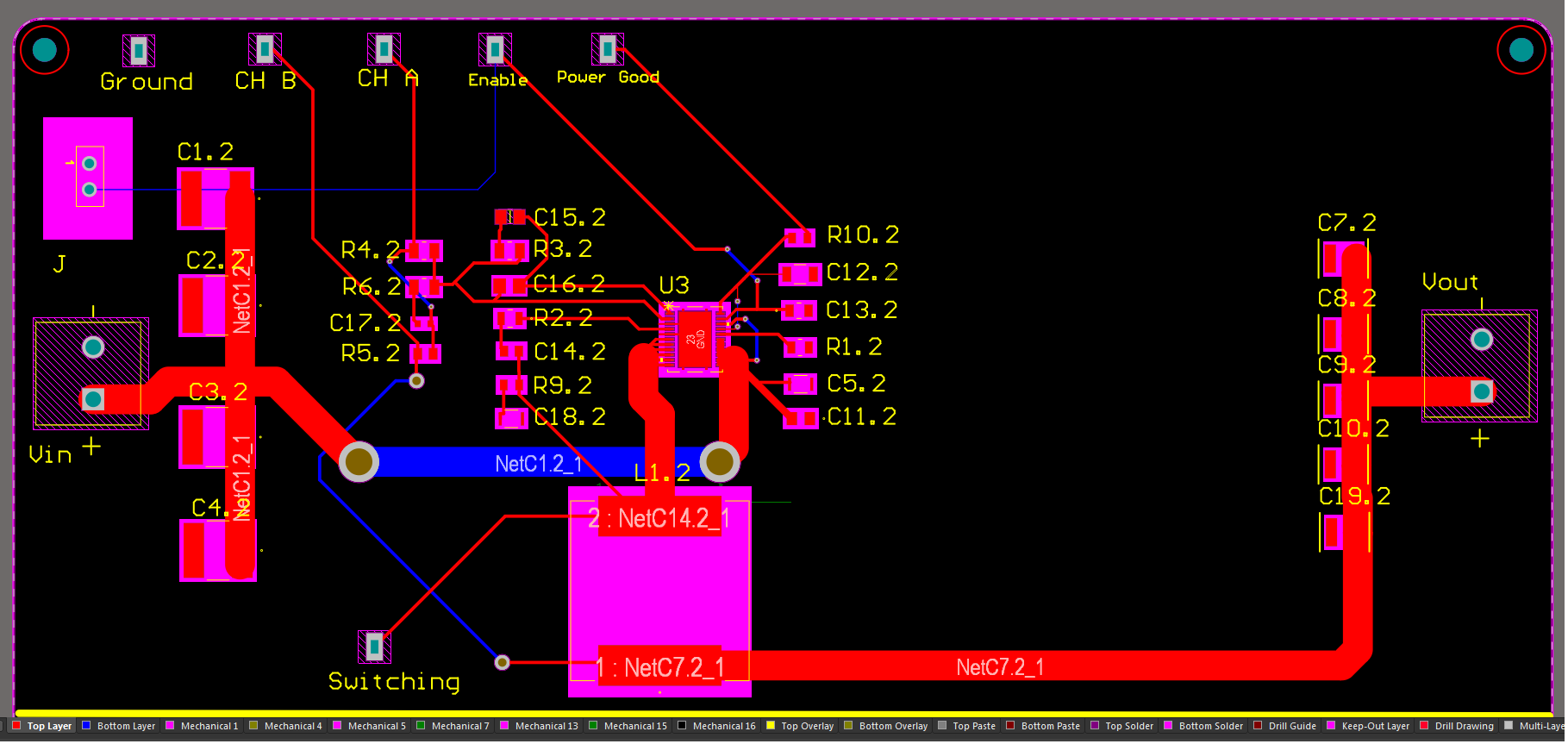
Unfortunately, my design is not working and I don't know why! I get zero output voltage when I have a clean 12V DC input from the supply voltage. I have no output voltage on Ch A and CH B.and can see 1V on Powergood pin and 5V on Enable pin. J3 is not connected (not shorted) in my design. I have attached the picture on my circuit along with my compensation loop calculation.

Does anybody know why this is happening?Thanks,

Babak

  • Babak,

    First off, I think your crossover frequency is too high.  Set at 100 kHz, the best the tool can manage is Fco = 75 kHz nd PM = 34.3 degrees.  You would be better of with Fco set to 50 kHz.  In that case, Fco = 49.8 kHz and PM = 56 degrees.

    More importantly, your layout looks very poor.  I am not surprised at all you are having issues.  You will need to closely follow the datasheet layout recommendations.  If you provide your actual layout files, I can comment further .

  • I used the Cross over freq and PM values that are recommended in the compensation tools (1/5th to 1/10th of switching freq Mine is 500kHz).

    I didn't know I have to follow the datasheet layout! I would love to know more about my layout and why it is poor. Here is my layout file. Is this fine or you need the actual Altium files?

    Thanks for your help,

  • Babak,

    Altium files would be great.  If you don't want to post them, you can email j(dash)tucker(at)ti(dot)com.

    1/5 to 1/10 Fsw is a good general rule of thumb so as not to ever get close to 1/2 Fsw.  However in this particular case you have to be mindful of the power stage gain and phase characteristics and also the limitations of the error amplifier and the calculation method of the tool.  I just noticed that your Fco an PM were not close to your specification and lowered the Fco until requested Fco and PM matched the calculated values.

  • Babak,

    I reviewed your design.  The circulating power loops are too long and especially the input capacitors are not close enough.  The data sheet has a detailed PCB example you should follow:

    I will close this thread for now.  Please feel free to contact me directly if you need additional assistance.  

  • Thanks John for your time.