Other Parts Discussed in Thread: MSP430F5529, IPG-UI,
Reported issue:
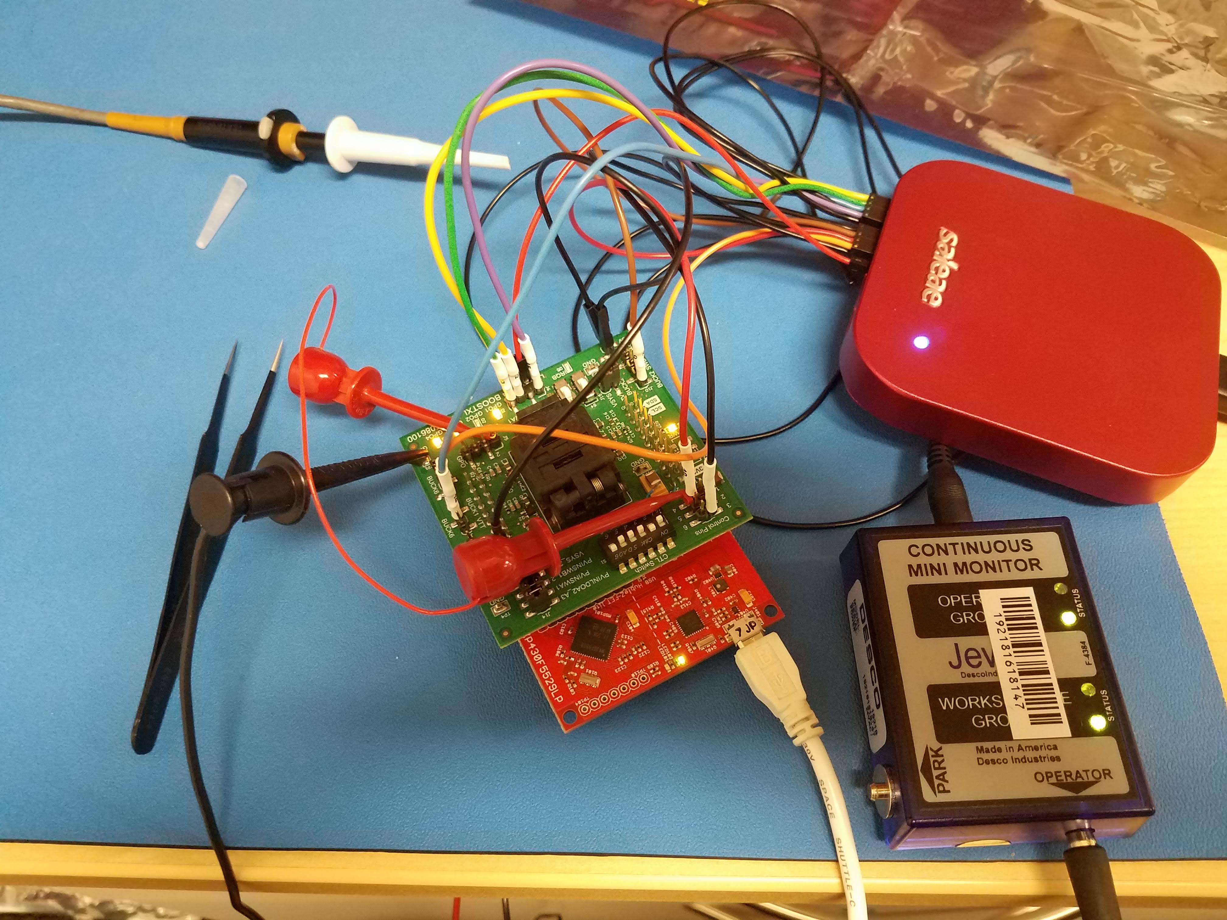
Customer is using BOOSTXL-TPS650861 + MSP430F5529 to program TPS65086100 units to match TPS6508640 OTP using
They are able to complete the programming, including up to "(5) Check" in the GUI with no issue, but when measuring the device they found the following behavior:
Note:
- CTL1 H
- CTL2 L
- CTL3 H
- CTL4 GPO1
- CTL5 H
- CTL6 L
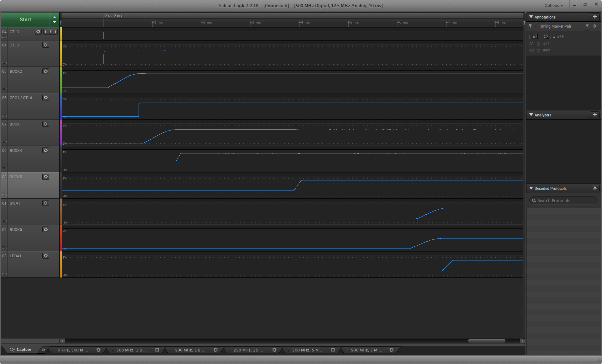
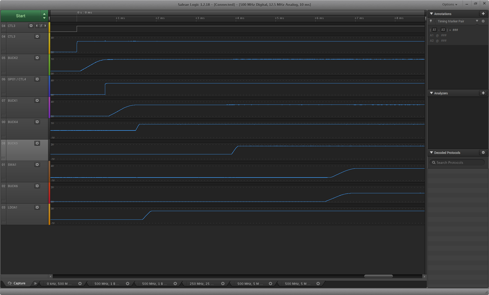
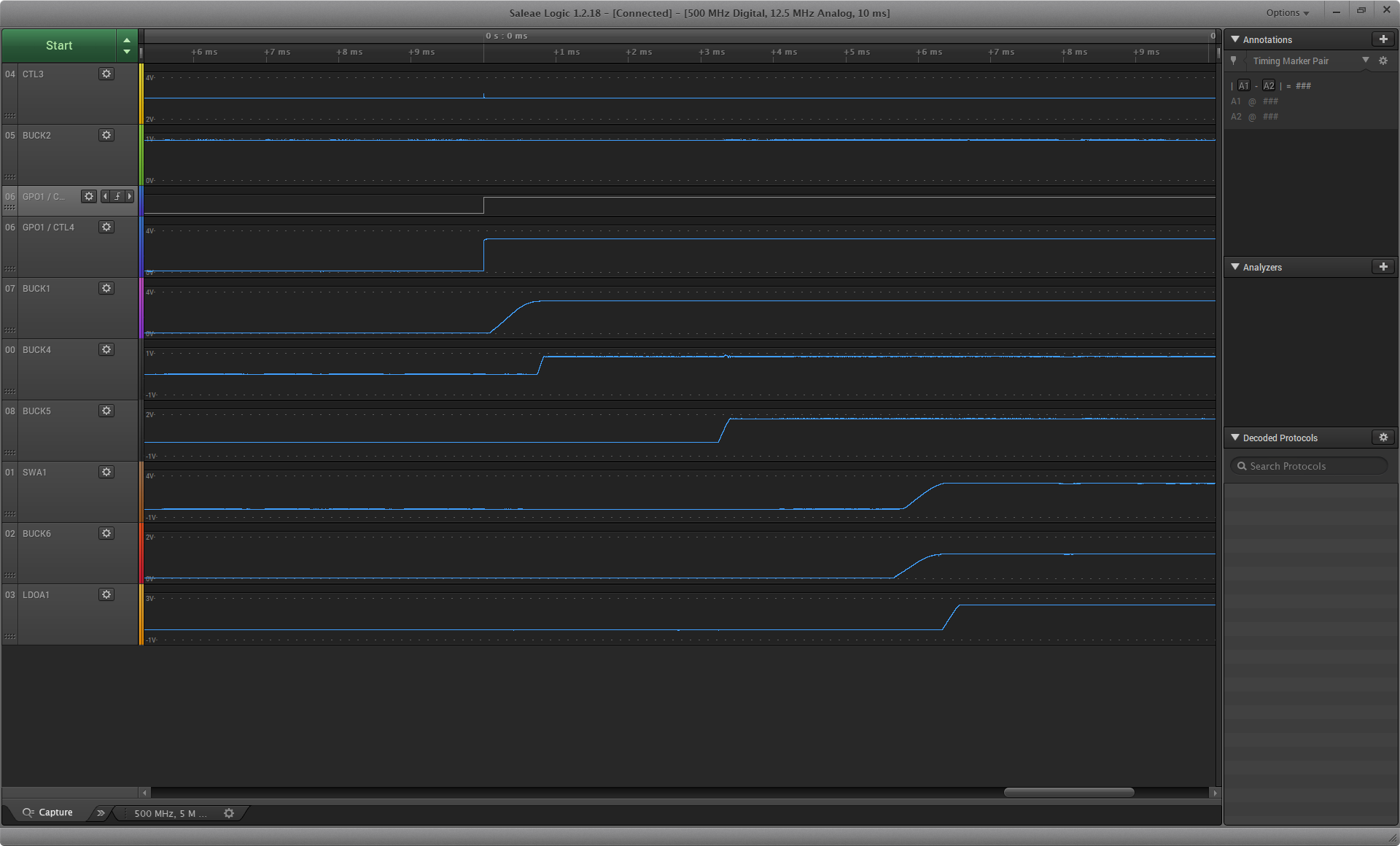
- They observe SWA1 enabled 120 ms after BUCK6, but TPS6508640 datasheet shows them enabled at the same time.
- BUCK6 and VTT change from 1.35 V to 1.2V after about 240 ms
- LDOA1 is enabled 500 ms after BUCK6. Changing it to BUCK4_PG shows no improvement
- They cannot find SWB2 in the Excel file?
[Scope shots provided by email]