This thread has been locked.

If you have a related question, please click the "Ask a related question" button in the top right corner. The newly created question will be automatically linked to this question.

PMP8740

Other Parts Discussed in Thread: UCC28180, PMP8740, UCC28950

Dear Roberto, 

At the time of testing I am bypassing Q12-Q31 MOsfet bank by putting wire link from C53 to J8 +, I have connected dcdc card to simple rectifier card and giving 12V to VCC_FB on J5 connector from external power supply. Now in this case I get stable 54V output when I gave 190VAC from variac. but my external power supply get loaded and input current I got from ext. power supply is around 1 A. 

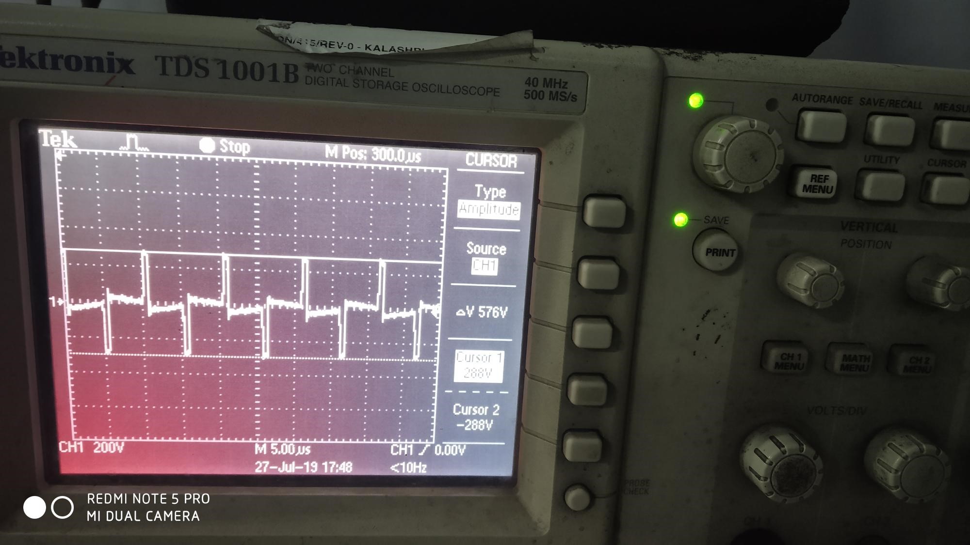
Also the waveform of T4 primary winding are like attached snapshot. are they ok ?  

  • Dear Anjana,

    The second waveform is correct, because there is no load on 54V (isn't it?) and therefore the feedback loop is closing the driving pulses.

    BTW, what is the first screenshot? Is it the T4 primary voltage at lower VAC?

    Second: at 12V the current consumption is too high: it should not be 1A; it will be 1A only when the fan is supplied at maximum RPM and all housekeeping is supplied at nominal load (so uC running, display on, backlighting on and top-speed for the fan).

    Thanks,

    Roberto

  • Hi Roberto,

    Yes another waveform is T4 primary at lower input voltage.  But my previous waveforms were much clear with lesser spikes inbetween two zero ( ref line of oscilloscope channel) crossings, also when feedback get closed at the same channel reference line you can see slope like line ,previously i got it very straight horizontal line.

    Regarding to external ps current, today i found that communication ic was dammaged.

    Anjana  

  • Dear Roberto, 

    here I am attaching previous and recent waveform of T4 primary winding, please check and tell me is recent wf correct? or something is wrong with it.

    Also, if I want to use IXFP72N30X3 mosfet in place of synchronous rectifier what changes I should  do in gate driver circuit?

    Thanks, 

    Anjana

  • Dear Anjana,

    I am not sure why the two waveforms are slightly different: can it be that in one situation the sync. rectification is not active? In this case, a small magnetizing current will flow on primary side (since the primary winding is not open during Toff but shorted) and therefore the voltage will be different, but I cannot confirm it.

    Regarding the MOSFET IXFP7xxx, this is a slower switch compared to the original one, so, please, double check that the extra turn-on delay (here 86 nsec) is not impacting the efficiency (you will see this by watching the output voltage of the current sense transformer (T1); this voltage can be seen across R34; if you have cross conduction, you will see voltage spikes on R34.

    Regards,

    Roberto

  • Dear Roberto, 

    So which MOSFET will suits there if my output voltage is 58V.

    I have check external power supply current by removing external load from +5V ( I have put 350mA external load on +5V to improve sw node voltage, as I have not interface uc card and LCD card) and It is noticed that current from external 12V PS current remains 1.2A as output voltage get stable at 54V, ideally when output voltage get stable at 54V external 12V  supply current should come down to 0.3A.

    I checked PWM ic it gives +5V reference , gate pulses are OK. also gate drive pulses from gate driver ics are also OK.

    why circuit sinking this much of current?

    Anjana 

  • Hi Roberto, 

    TI organised the TI Automotive Techday in Pune, India on 8th Aug 2019, will you be there

    Anjana

  • Hello Anjana,

    I would suggest to select a 300V FET, for example on of the following:

    Regarding the current consumption, on the schematic of the PFC stage of my design I wrote a list of power consumptions, which I report:

    Main power consumptions:

    PFC Stage:

    UCC28180, 200mW (driver included)

    DC/DC Stage:

    Relay: 400mW

    FAN: 1.7W

    LCD backlight: 600mW

    Various: 1W

    Needed Auxiliary: 6W

    Total: 10W

    If you removed some loads, you should have lot less than 6W power consumption.

    Therefore I suggest to check the temperature on several points, and see if there is anything hot.

    Best would be to have a infrared thermal camera.

    Regards,

    Roberto

  • Hi Anjana,

    No, unfortunately I will not be there.

    I will start my vacation on 8th of August and will be back on 1st of September.

    Regards,

    Roberto

  • Hi Roberto,

    When i am powering dcdc card from rectifier, output voltage get stable at 190VAC, primary waveform also seen as expected , but when i increase input voltage above 190VAC primary waveform get disturbed and input current of extermal 12v power supply also stays at around 1- 1.2A.

    Gate dives and other waveforms are as expected. , There is no other load on 5v supply.

    Why this is happening?

    Anjana

  • Hi Anjana,

    That sound me really strange.

    The rectified 190VAC is also supplying the auxiliary power supply. I believe you are supplying your board through 12V. In this case you should disable the internal Flyback auxiliary PSU, placed on the Boost PFC board....did your already made it?

    If this is the case, then I think there is a damaged component somewhere. You should see it with an infrared thermal camera.

    If possible, by the way, send me a block diagram, showing all connections on the system you have by now.

    Best regards,

    Roberto

  • Hi Roberto,

    Yes i have disable smps on pfc hence i am powering up 5v and from external12v power supply.  

    Something is damaged or not working properly for sure, because of which i m getting 1A current from  12v supply. And hence i m not able to go beyond 190VAC. But who is damaged?

    Anjana

  • Dear Roberto, 

    Here is attaching block diagram of connections and modifications done on PFC board and DCDC board.

    Please help, 

    Anjana

  • Hello Anjana,

    Please try to do a typical troubleshooting, by watching the current consumption on 12V rail, and disabling step by step several section of the power supply.

    This way you should be able to understand where is the defective component.

    Tomorrow I will start my vacation and I will be back on 2nd of September, but I will read emails time to time, so my response maybe delayed.

    Best regards,

    Roberto

  • Dear Anjana,

    It looks like this setup and the connections are correct, so, please, troubleshoot your control section, because there must be a defective component.

    Best regards,

    Roberto

  • Ok Roberto, I will check it again. 

    Sorry for disturbing. Enjoy your vacations.

    Anjana

  • Dear Roberto,

    I have solve problem of increasing input current, it was because of non-isolated scope connected across Transformer primary.

    Now I am facing new problem while testing, that , when I gave ac supply upto 190VAC output is stable at 54V , input current of both AC supply and external 12V supply are as expected. but when I start to increase AC Supply voltage beyond 190VAC some distortion like noise starts, input current (Ac supply & External 12v supply) starts decreasing, and gate pulses get disturbed and come and go.

    another problem is,  when I give ENA_FBP4.7 Signal, the voltage at pin SS/En starts rising from 0.7V to 1.3V and after 1.3V U2 enables. this happens every time when I gave enable pulse. Otherwise on other board this SS/EN pin voltage is 4.23V stable as soon as enable pulse given. I checked dry solder around enable signal and SS/EN pin.

    Plz help.

    Thanks, 

    Anjana

    .     

  • Dear Anjana,

    I suspect that your 12V  external supply is getting disturbed from your AC source: is this source isolated?

    If not, the 12V source probably doesn't like to be connected to AC mains (mainly because of the internal feedback loop, which is sensitive).

    When I test my system and I connect the converter to mains (and disable the PFC stage) then I always use the auxiliary power supply of PMP8740, in fact to avoid to connect an external power supply to live mains terminals.

    When I test my system, only if the DC/DC is active, with a DC power source, then I connect the ground of DC source to the ground of DC/DC of PMP8740, and also the ground of the external 12V power supply to the ground of DC/DC pf PMP8740. This way all grounds are tied together.

    If you are testing only the DC/DC section of PMP8740, can you please use a DC power source and check again if you have disturbances or noise?

    Regarding SS/EN pin, according to the datasheet (paragraph 7.3.14) the voltage at the end of SS phase should be  > 3.7V, so I believe there is a problem with that controller.

    Best regards,

    Roberto

  • dear Roberto,

    I use separate DC regulated power supply for 12V and the ground of both regulated power supply and PMP8740 dcdc board are tied togather. 

    This SS/EN pin phenomena is seen in two boards. one board is ok giving expected operation. 

    In problematic board SS/ EN pin voltage and COMP voltage are fluctuates anywhere from 0.7 to 4.5V. here if I put only C8 and removes( Q1, Q3, R108, R33, C11) then ss/en voltage remains stable. Plz note all those components are externally checked OK, on board checked OK.

    Anjana

  • Dear Anjana,

    So you have a separated DC regulated power supply, set to 12V, with its ground connected to the DC/DC stage (let's call it PSFB) of PMP8740. Then the PSFB input voltage comes from a rectified (plus bulk electrolytic capacitor, right?) AC source that is the mains voltage, correct? Do you have an isolation transformer between the rectifier and the PSFB? If not, please consider that the ground of PSFB will be "jumping" up and down with the mains potential, which can affect the regulation of the DC power source. This can also generate perturbations to the digital signals, like the ENA_FB P4.7.

    Please let me know.

    Regards,

    Roberto

  • Hi Roberto,

    Can you give me T4 transformer construction details?

    Anjana

  • Hi Roberto,

    Why that isolation transformer is required between rectifier and psfb?  Because on the pfc board there is only isolation transformer in smps section which separates GND-P and GND-S. Here i use separate regulated dc power source. Will this still cause grounding problem?

    Anjana

  • Hi Roberto,

    Another problem arises yesterday is , at the time of testing on only 12v supply ( no ac supply) , normally when dcdc stage enables i got 2v at output connector, but yesterday i saw, as i enables dcdc stage output voltage become 0v and it became 2v when dcdc get disable.

    Also i am getting 3.5v at R9 and R10. Which is 0.5v on ok board. In this case sunchronus rectifier is also turns on.

    Anjana

  • 2705.145400-a_eng.pdfHi Anjana,

    I attached the datasheet of the transformer T4, provided by the German manufacturer Kaschke.

    I don't have the details regarding the type of the core, while the number of turns is Np = 19t and Ns = 2t; Kaschke designed and provided the samples for free, therefore I don't have and we agreed to not disclose the complete construction details.

    Best regards,

    Roberto

  • Hi Anjana,

    Actually I don't have any answer for this, sorry :-).

    Regards,

    Roberto

  • Hi Anjana,

    The isolation transformer can be placed between the rectifier and mains, or between the DC power source and mains.

    With the first connection, you can attach non-isolated voltage oscilloscope probes to the DC/DC primary side, because the ground is isolated.

    If you don't use any isolation transformer, the ground of DC/DC converter will "bounce" from the terminal "line" of the mains connector (during positive half-cycle) to the terminal "neutral" of mains, during negative half cycle.

    Maybe if you attach a detailed drawing of your setup, I can clarify it better.

    Thanks,

    Roberto

  • Hi Roberto,

    For my design my turns ratio calculated as 5.4, and so i chose 15turns and 3 turns for pri and secondary resp. I use sandwich  winding, hence my layers from inner to outer are pri, sec,sec,pri. Pri gauge is 120x0.1mm litz wire

    Now i wish to increase no of strands of pri winding wire, and if i use  available wire at me 220x 0.1mm litz wire then winding is not accomodating. Hence my tx manufacturer ask me to change turns ...so can i select 10 and 2 turns  for pri and sec resp.

    Also can i use primary winding as a single winding instead of sandwitch .

    W

  • Hi Anjana,

    Please check that by using 10 turns on primary side the magnetizing current is not too high (you can check it by using the UCC28950 calc-sheet).

    Both sandwich and single winding structure will work for a PSFB, because the leakage inductance is also leveraged from primary side.

    By having a look to my transformer, I confirm that this is built with single winding.

    Regards,

    Roberto

  • Dear Roberto,

    my calculated current values with 15no turns of T4 primary are as follow

    NO of turns: 15; Lmag: 1.4mH; ΔILMAG: 0.96A; Ipp: 8.9A; Imp: 6.5A; Imp2: 8.84A; Iprms1: 4.8A; Iprms2:3.01A; Iprms: 5.7A; drain current Id: 13.41A; Shim inductance LS: 9.2uH

    Where as if I reduce no of turns to 10nos then 

    NO of turns: 10; Lmag: 0.67mH; ΔILMAG: 2.01A; Ipp: 9.5A; Imp: 6A; Imp2: 9.26A; Iprms1: 4.8A; Iprms2: 3.17A; Iprms: 5.8A; drain current Id: 14.19A; Shim inductance LS: 7.91uH

    is this OK? will  ΔILMAG affects any other parameter  like current limit or anything else?

    Thanks, 

    Anjana

  • Dear Anjana,

    I believe both calculated values are fine. With 10 turns you get a bit higher RMS currents, which will involve slightly higher conduction and switching losses (because also peak currents are higher), but nothing dramatic.

    Increased delta-Imag will impact the cycle-by-cycle current limit on primary side, and the slope compensation (with higher slope on the mag-current, you need less slope compensation, but it's marginal).

    Best regards,

    Roberto