This thread has been locked.

If you have a related question, please click the "Ask a related question" button in the top right corner. The newly created question will be automatically linked to this question.

LM5175: Diode emulation not working in boost mode

Part Number: LM5175
Other Parts Discussed in Thread: LM5176, INA181

Hi 

I have the same problem as here : https://e2e.ti.com/support/power-management/f/196/t/648997?LM5175-LM5175-Synchro-Management-of-Boost-Highside

My project : Input 12-15 V (battery); output 13.8/14.7 V into antoher battery ; 30 A max. (battery charger). IC : LM5175. 

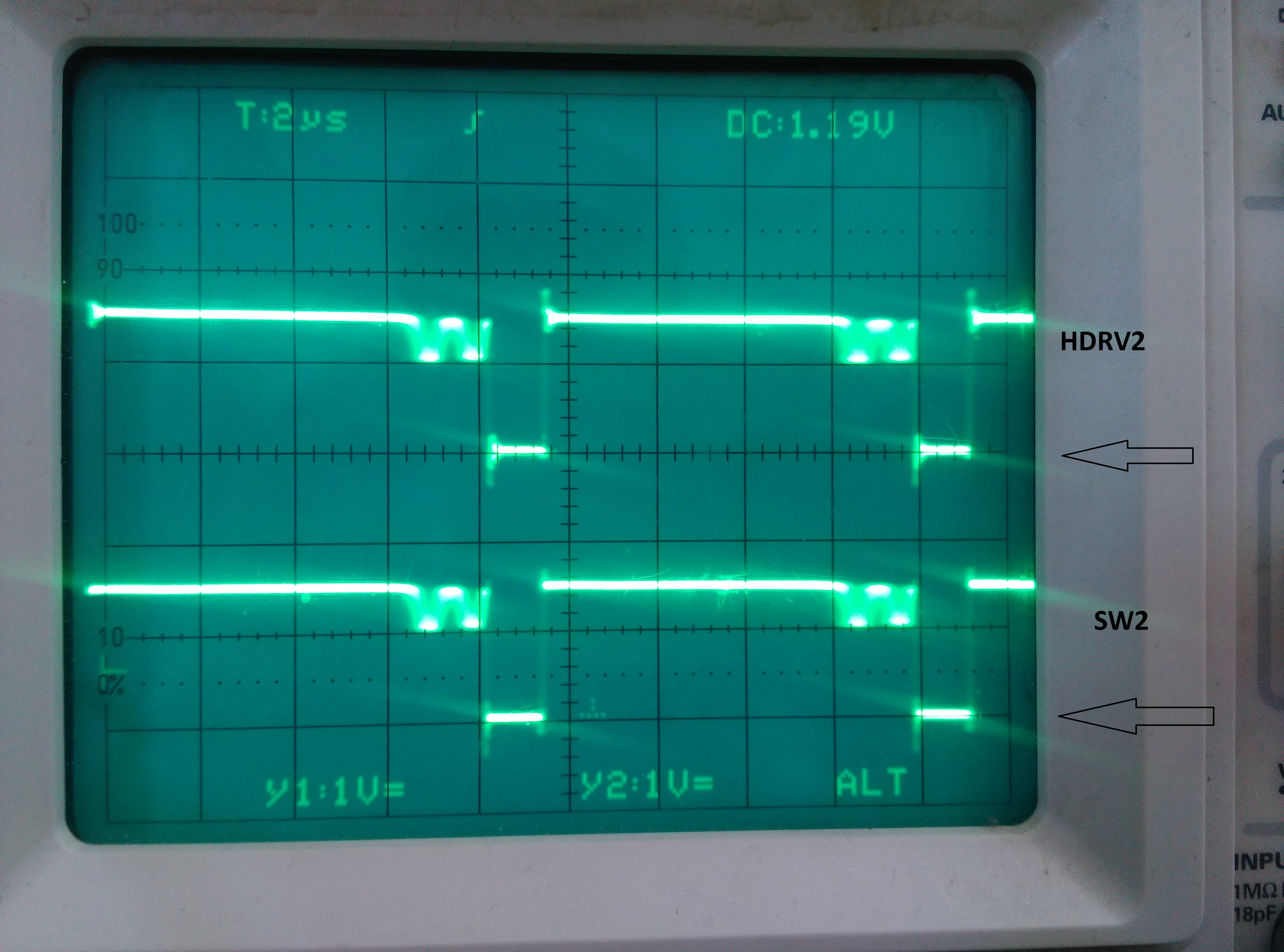
The problem is that high transistor of the boost side of the bridge it is not switched by the  driver. It can not work as a diode  , given the output current needed. So the diode emulation feature is a must. But it seems to not working as expected. 

In DCM mode the high transistor of the boost side of the bridge is driven only in specific conditions, namely :

  • when the converter works in buck mode : the gate is driven 
  • when the converter works in buck-boost mode : the gate is driven only on half the switching period
  • when in boost mode: the gate it is not driven at all (works as diode )

Can the problem be because the IC does not sense when the current through inductor falls to zero ? Also regarding this, how does the IC senses the current through inductor in DCM mode?

How does the IC senses the current through inductor in boost mode ? Because in boost mode there is no current at the common source shunt. 

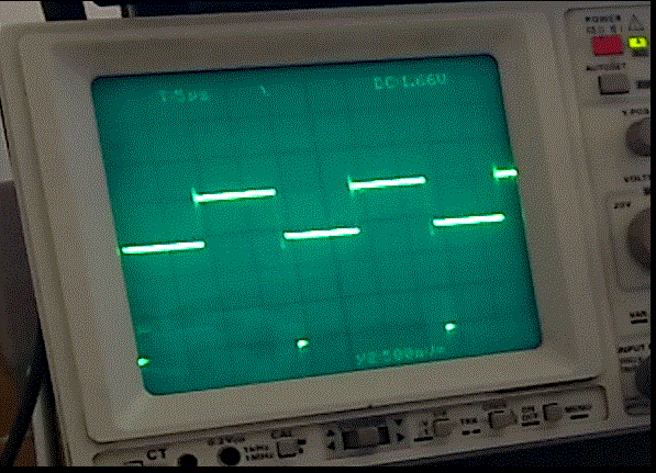
See photo (waveform : HDRV2 referenced to PGND) 

  • Hi Ionut,

    Thank you for using the LM5175.  Not sure if I really understand your question.  It is not correct that "when in boost mode: the gate it is not driven at all (works as diode )".   Actually, HDRV2 will still drive in DCM.  It is only turned off off when the current cross zero and intend to reverse the direction.  

    In the boost mode, the zero current detection is achieved by monitoring SW1 and VISNS pin.  The reverse current will put SW1 voltage higher than VISNS.

    Thanks,

    Youhao Xi, Applications Engineering

  • I came back with another photos  : 

    below you have : power supply : 12 V input; 

    output voltage 13.8V 

    in first photo you can see SW2 and HDRV2 voltages referenced to ground. They are the same. Meaning the upper transistor does not switch

    The arrows indicate the ground / zero voltage level

    In the second photo you can see HDRV2 and BOOT2 voltages referenced to ground. So bootstrap circuit is ok. 

    Also 

    look the power supply  (when measuring SW2, HDRV2) 12.4 V / 1.8 A

  • Also, is there any case when HDRV2 is not complementary to LDRV2 (forced CCM) ?

  • Thank you for the pictures, but I don't see any difference between your 1st and 2nd scope pictures, in which you said the 2nd was about HDRV2 and BOOT2.  Did you post a wrong picture there?  Anyway, the 1st picture shows DCM: the resonance at the end of the waveform of SW. 

    (HDRV2-SW2) and (LDRV2-GND) will always be in complementary in CCM.  The complementary will be lost in DCM, because the HDRV2 would turn off earlier.

    I am afraid if the high side driver HDRV2 is damaged somehow.  

    Thanks,

    Youhao 

  • We have encountered this behaviour on several boards with lm5175 and lm5176. And strange enough this happens only when the load is a battery or a resistance. With electronic load hdrv2 does switch.

    I don t think the driver inside LM5175/LM5176 is faulty because under certain conditions we can see gate pulses on HDRV2. It is something with the driving logic part.  

    Can it have any influence the fact that i use SS pin to limit the current and not the COMP pin?

    Also how can I share with you the schematics and  a video with you, in privately?

  • The purpose pf the photos was to show  you that HDRV2 is not equal with SW2+Vcc , despite the fact this voltage does appear at BOOT2. How can this happen for a high side driver? Or can this be because of the proprietary circuit of the gate drive  

    which works even if one leg of the bridge does not switch in order to recharge the boot cap ?

  • Hi Ionut,

    I think your control of SS pin voltage  may explain.  If the SS pin is pulled low, the IC may think the circuit still in soft-start phase, and the HDRV2 is hold off on purpose to prevent back flow current.  Please release the SS pin and see if the issue is resolved.

    In our circuit after starting up, the high side driver boot cap should always be held high even when the leg is not switching. 

    Thanks,

    Youhao

  • So I can not externally  discharge  SS capacitor  to limit the output current?

    Because the datasheet gave the impresion I can do that : "The soft-start pin is also discharged

    when the converter is in hiccup mode current limiting or in thermal shutdown. When average input or output

    current limiting is active, the soft-start capacitor is discharged by the constant current loop transconductance

    (gm) amplifier to limit either input or output current" .

    My output current control loop measure a shunt in series with the output, it is amplified by an INA181 and the amplified signal is compared with my reference signal which sets the desired output current. The amplifier which makes the comparison pulls down the SS pin, hence obtaining the desired output current.

    For controling the output current is mandatory to use ISNS+/ISNS- inputs ( and thr asociated control loop ) ?

    Or can I put the output of my amplifier to pull down the COMP pin instead of SS ?

  • If the IC think is in SS why does it switch LDRV2 ?

    Anyway we tested without our current control loop; the SS pin is left free; but still this behaviour occured

    IN DCM there is no gate pulse on HDRV2 transistor for a 12V input 14.3  V output. The current flows through the transistor's body diode. 

    HDRV2 starts to switch at about 13.8V (as in my very first photo) ; and at about 16 V it is fully turned on ( the current flows through HDRV2 transistor)

  • No you should not.  The SS pulldown is intended for the internal average current limit circuit and the SS cap also serves as the compensation element for that circuit. Once it is in action, the internal circuit knows and the SS ready signal is not overriden.  If you separately pulldown the SS externally, the SS ready state will be reset, and you can get into the situation that the HDRV2 stays off.

    Thanks,

    Youhao

  • As I said :  we tested without our current control loop; the SS pin is left free; but still this behaviour occured

    IN DCM there is no gate pulse on HDRV2 transistor for a 12V input 14.3  V output. The current flows through the transistor's body diode. 

    HDRV2 starts to switch at about 13.8V (as in my very first photo) ; and at about 16 V it is fully turned on ( the current flows through HDRV2 transistor)

    Do you have any advice for this?

  • I have tested out EVM and the HDRV2 only switches off when the current try to reverse direction.    May I ask you to set the IC to forced PWM mode and see if the HDRV2 can turn on in condition?  Then we can tell if this is caused by the DCM mode setting or not. 

    Thanks,

    Youhao

  • Hi Ionut,

    Can I assume the issue is resolved?  Let me close it here but you can re-open it by adding a new post.  If you have any updates, please let us known.

    Thanks,

    Youhao 

  • Unfortunately due to deadline pressure we were forced to abandon the LM5175/6 solution, and currently we are trying another IC.

  • Thank you for the update, and sorry to hear.  Let's close this thread here, and contact us if we can be of assistance in the future.

    Best Regards,

    Youhao