This thread has been locked.

If you have a related question, please click the "Ask a related question" button in the top right corner. The newly created question will be automatically linked to this question.

TPS74801: TPS74801

Part Number: TPS74801

Hello,

 have question regarding a power designer simulation using a TPS74801.

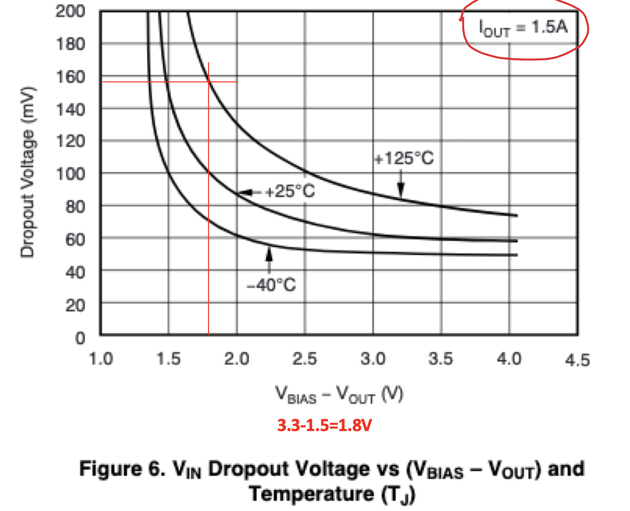
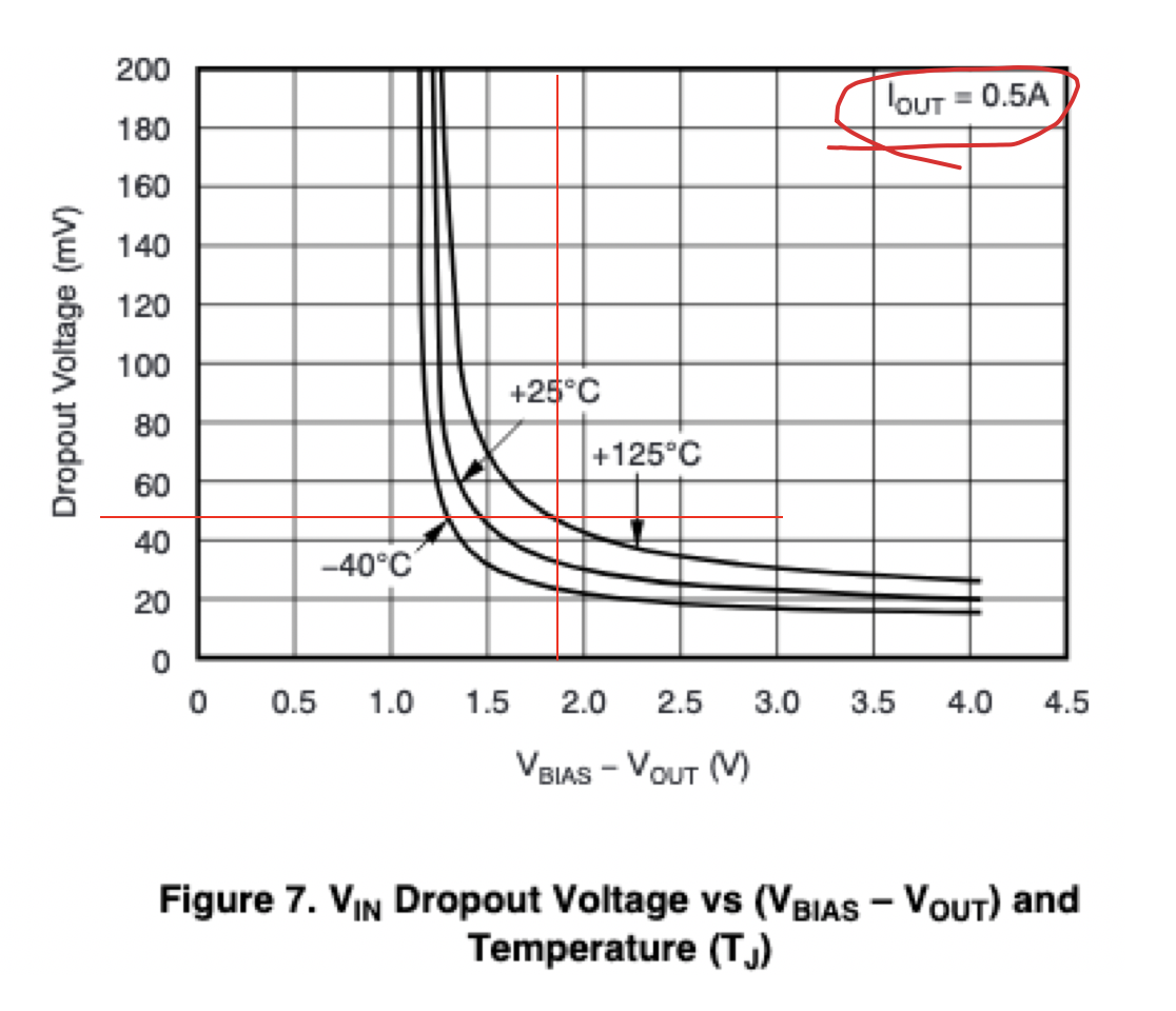
My Power Designer settings as following: Vin_min=1.69V; Vin_max=1.71V; Vout=1.5V; Iout_max=0.5A;Max Ambient 55C. 

I would like to set Vbias to 3.3V, to match my intended design configuration. For some reason the lowest value that available is 3.5V. 

Question, Why the lowest Vbias value is 3.5V? According to the part spec, a voltage applied to the Vbias pin could be as low as Vin + 1.65V. Even, as I understand that is not a recommended configuration.

Also, do you see any issues with my configuration?

Regards,

Alex

  • HI Alex,

    With VIN at 1.7V, and VOUT at 1.5V, for a maximum of 500mA and VBIAS at 3.3V, figure 6, on page 10 of the datasheet indicates that at 1.5A, the drop-out voltage (VDO) is ~160mV:

    The translates to an effective RDSON of ~106mOhms. if your max load is only 500mA, then your typical VDO is going to be ~53mV. Figure 7 on page 11 confirms this as shown:

    So at your load current with 3.3VBIAS, 1.7VIN and 1.5VOUT at 500mA, it looks like you are OK.

    I hope this answers your question

  • Hi Alex,

    To answer the Power Designer question, this is a simple  tool to help recommend solutions. From what I can see is VBIAS is optimized assuming you are using the maximum load current capability of the device.

    The datasheet has the information needed to ensure that the part works in your application.

    Regards,

  • Hi John.

    Thank you very much.

    One follow up question:

    1. Is there a way to predict drop at relatively lighter load, somewhere around 10 - 20mA

    Alex

    2. Why Power Designer does not allow

  • Hi Alex,

    1. For 10-20mA, the explanation I provided above applies. With VBIAS at 3.3 and a VOUT of 1.5V, the fully enhanced RDSON of the FET is 106mOhm so your VDO at these load currents would range from 1-2mV. This really only has meaning if your input voltage is falling (for example a battery).

    2. While the power designer does pull up some of our LDO's it is more focused on helping to better pick switching regulators. This tool uses simple parameters extracted from the datasheet and it by no means comprehensive.  This is why we have E2E so you can get answers to questions like this.

    I hope this helps.