This thread has been locked.
If you have a related question, please click the "Ask a related question" button in the top right corner. The newly created question will be automatically linked to this question.
Hello,
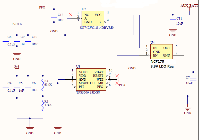
I am using the TPS3606-33 part in a battery powered embedded design. The schematic for the design involving the TPS3606-33 part is shown below.
For this design the VBAT pin is driven from the output of a 3.3V regulator U4. To conserve energy this regulator is normally disabled and is controlled by the 'PFO' output from U3 (TPS3606-33). So when VDD is 3.3V, VOUT will be sourced by VDD and the U4 regulator should be OFF. I am curious if it is OK to operate the TPS3606-33 part with the VBAT pin near ground (U4 disabled). I have noticed that in this mode where VOUT = VDD the VBAT pin pf U3 measures ~0.5V to ground which appears to be generated from inside the U3 TPS3606-33 part. I have confirmed this by lifting the OUT pin of U4 and the VBAT pin of U3 measures ~0.5V when VOUT = VDD.
So I would like to make sure that this approach of disabling the U4 regulator which drives the VBAT pin of U3 is acceptable for proper use of the TPS3606-33 part.
Thank you.
-Sean
Sean,
I don't see any issue since Vbat = 0V doesn't violate the ABS MAX rating however the Vbat functionality with not work unless Vbat pin is within the recommended operating range 1.5V to 5.5V. Also, I believe the difference in supply current when the LDO is enabled vs disabled is only 0.4uA however the current through R4+R2 to set the PFI threshold at the PFI pin plus the supply current of the inverter is much more than 0.4uA. I would recommend just simply connecting the LDO output to the Vbat pin so that Vbat is always operational if the case VDD (and PFI) suddenly fail, and remove the PFI resistors and inverter to save current. When the VOUT of TPS3606 is connected to VDD when VDD is high, the Vbat pin only consumes 0.1uA.
But to answer your original question, there should be no issue connecting LDO output to Vbat.
Hi Michael,
You make an excellent point regarding the fact that the circuit is consuming more energy to enable/disable the U4 (due to the current consumption of U7) v.s. just leaving U4 enabled all the time.
I also agree with your comments regarding power consumption of R4 and R2 for the PFI/PFO functionality. However this circuit needs the 'PFO' output to control the PLL state of an attached oscillator. Pin 3 of J4 in the schematic below is pulled low to enable the PLL of the oscillator and left to float high in order to disable the PLL. This part of the circuit was not shown in the schematic I sent. Below is a schematic showing this recent mod to the circuit which uses the 'PFO' line to control the MOSFET U11. Previously this MOSFET was controlled by a 3.3V regulator which would go out of regulation when the main batteries would fail and therefor disable the PLL for power savings. This approach however was problematic so I have recently made the hack shown in black. In the schematic I erased the connection between '3v3' and the gate of U11. So to achieve this 'PFO' line control of U11 I have to add the black wire shown in the schematic below and also remove the connection to between '3v3' and the gate of U11. So U11's gate is driven by the 'PFO' output of U3. When main batteries fall to just under 4.0V the 'PFO' line state will toggle and the PLL of the oscillator will be disabled. From my testing this seems to be working well.
The final hack I will make (as you suggested) is to remove U7 and connect U4's pin 3 'EN' pin to C11 or AUX_BATT. This way the VBAT pin of U3 always receives 3.3V as long as the "AUX_BAT" is connected which should always be the case. I agree that for the switching logic of U3 to function properly there should always be 3.3V applied to the VBAT pin. Below is text taken from the TPS3606-33's data sheet on page 5 specific to the backup-battery switchover condition. It makes sense to me that in order for this logic to work VBAT needs to be set properly.
"VBAT only connects to VOUT (through a 2-Ω switch) when VOUT falls below V(SWN) and VBAT is greater than VDD."
Thank you again for your help and input.
-Sean
Excellent and please let me know if you have any additional questions or if you have any issues with TPS3606.