This thread has been locked.

If you have a related question, please click the "Ask a related question" button in the top right corner. The newly created question will be automatically linked to this question.

TPS63060: Chip damage issue

Part Number: TPS63060

Hello

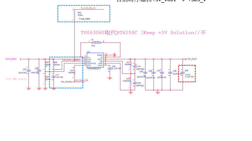
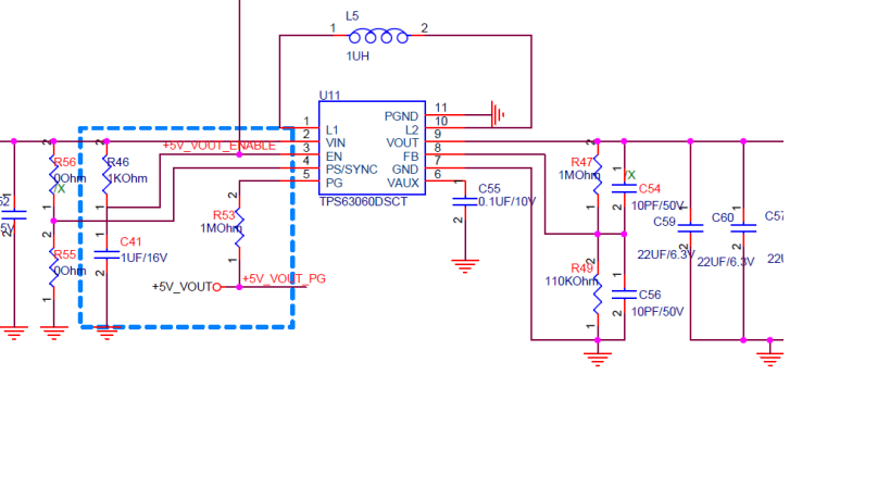
       Customer meet IC has no output damage issue while Burning machine testing long time. They change R55 0hm to R56 for PWM mode.  R49 change to 120kohm. Has any risk for the design? Thank you. 

BR

Patrick

  • Hi Patrick:

    May you help to describe the " Burning machine testing long time" with more details? What's the temperature and the Vin, Vout, Load conditions?

    And did the converter keep enable? Or in other way, is the input voltage constant and stable? If not, please provide how it changes.

    It's better to make the system and test clear, then could we check if there is any risk and how to avoid them. Thanks for your understanding.

  • Hello

    Dear Minqiu

              Could you help provide comments based on below condition? Thank you. 

    Vin 5V (Power Bank provide 5V power source)

    Vout =4.67V

    FB 1Mohm &120Kohm

    dynamic load condition: 0.05A~1.45A, interval 1s; slew rate 2.5A/us

    Enable pin is connected to VIN, PWM mode, temperature is 25°C, 

    CAUX 0.1uF/10V 0402


    BR

    Patrick

  • Hi Patrick:

    The Cout is recommended with 3*22uf 16V capacitance. There will be a obviously DC-bias for MLCC. Please make sure it has enough effective capacity.

    And it's better to share the layout and waveform with me, to check if there is other obvious risks. 

  • Hello Minqiu

    DC bias for MLCC X5R

    22uF/16V capacity is 12.843uF while at 5V

    22uF/6.3V capacity is 12.837uF while at 5V.

                    Could you help double confirm  has any risk for schematics and layout? Thank you. 

    https://e2e.ti.com/cfs-file/__key/communityserver-discussions-components-files/196/0724.1753.7z

    BR

    Patrick

  • Hi Patrick:

    It's glad to see you check the capacity of the caps.

    Unfortunately, we failed to open the schematic and layout. It noted:"Database is locked for exports. Need password to open". Do you have alternately way? Or just screen shot?

  • Hello Minqiu

               Please refer to attached again. It should no setting password to open it. Per schematics, modification is below. 

    R49 110Kohm change to 120Kohm,R55 0ohm move to R56 PWM mode

    https://e2e.ti.com/cfs-file/__key/communityserver-discussions-components-files/196/TPS63060.7z

  • Hello Minqiu

           Screen are below. Thank you. 


    BR

    Patrick


  • Hi Patrick:

    Thanks for your supplement. 

    According to your layout, the package of the Cout, Cin is large. It's recommended to add a small size and smaller value cap close to the IC to reduce the parasitic parameter.Below is the example showed in datasheet.

    And the C56 is recommended for PFM mode. If you choose disable PFM, you don't need it.

  • Hello Minqiu

               if  Cout, Cin use original value and not use  small size and smaller value cap, Does  the parasitic parameter of bigger Cout, Cin will cause any risk for the design due to the current testing has no no problem? 

              If add C56 on PWM mode, has any side effect for it? Why it is recommend to add C56 for PFM mode? Thank you. 

    BR

    Patrick

  • Hi Patrick:

    It's better to measure the waveform of L1, L2, Vout, to check the switching noise. ( We have heard a lot of customer damage their circuit with improper layout.)

    For the C56, as datasheet mentioned, "Place a small capacitor (10 pF) in parallel with Rdown when using the power save mode and the adjustable version, to provide filtering and improve the efficiency at light load." If without this for PFM, there will be more noise and less efficiency.         Which mode do you want? I'm little confused.....

    Besides, I forgot to check with the inductance. May you share the part number or datasheet of the inductance with me? If there is no enough current capability of inductance, it also will damage the converter when saturated.

  • Hello Minqiu

                        if add C56 on PWM mode, has any side effect for the design? We will send inductance datasheet later. Thank you.

    BR

    Patrick

  • Hi Patrick:

    Thanks for your supplement.

    The C56 will influence to the controller loop. But generally speaking, for such value it won't influence too much.

  • Hello Minqiu

            Attached is L1/L2/Vout testing waveform and inductor datasheet . 4.8Vin, DC load 1.45A-0.02A. slew rate 2.5A/us. 


            Could help review the waveform has any risk to damage circuit?  Thank you. 

    L1-L2 test waveform.pptx

    PCMB041B-1R0MS.pdf

    BR

    Patrick


  • Hi Patrick,

    The waveforms look good, and the inductor is properly sized.

    Best regards,
    Milos