This thread has been locked.

If you have a related question, please click the "Ask a related question" button in the top right corner. The newly created question will be automatically linked to this question.

TPS23754: Can not pass detection

Part Number: TPS23754
Other Parts Discussed in Thread: , TPS23752

Hello,

I would like to ask You for help with our design including TPS23754. This design is following TPS23754EVM-383 EVM, but to be on a safe side I include our schematic (please ignore the blue comments, they are only for picking smaller components in further implementation).

PCB_POE_TPS23752.pdf

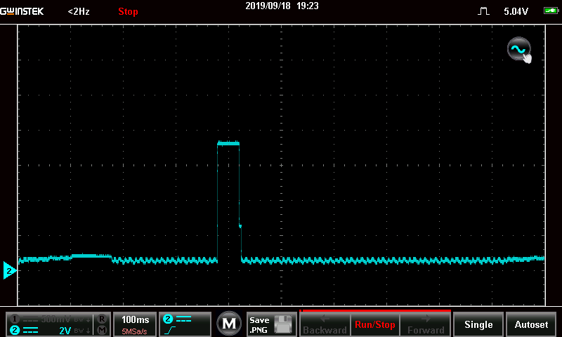
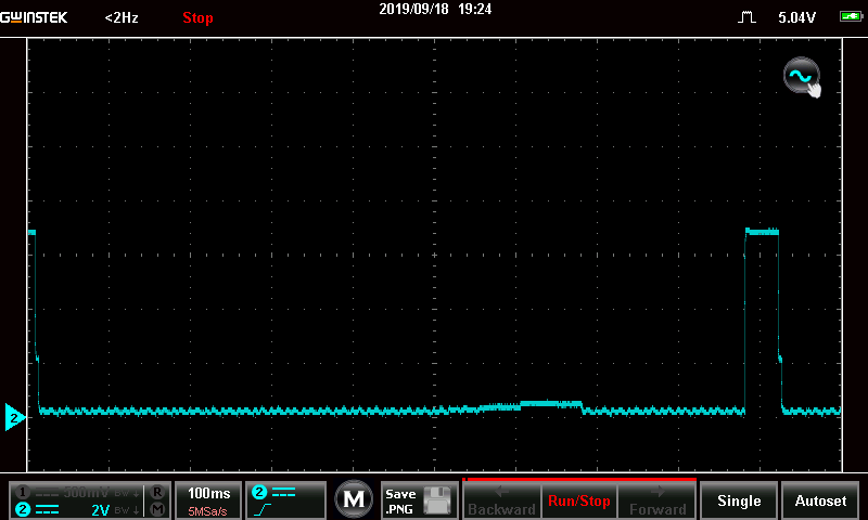
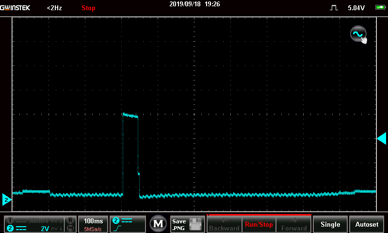
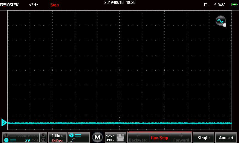
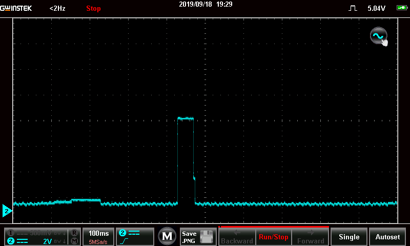
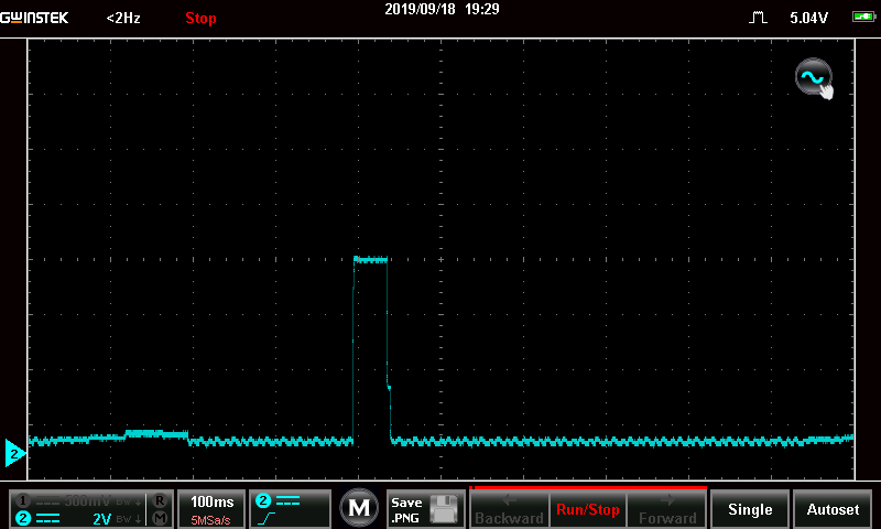
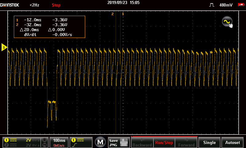
Our problem is that we cannot pass detection and we can not figure, what went wrong because we followed reference design. Here I add also measurement of VDD-VSS from capacitor C2. It seems that PSE is trying to detect something and it is not getting any answer. We are using this PoE Injector: PSE802G-30W.

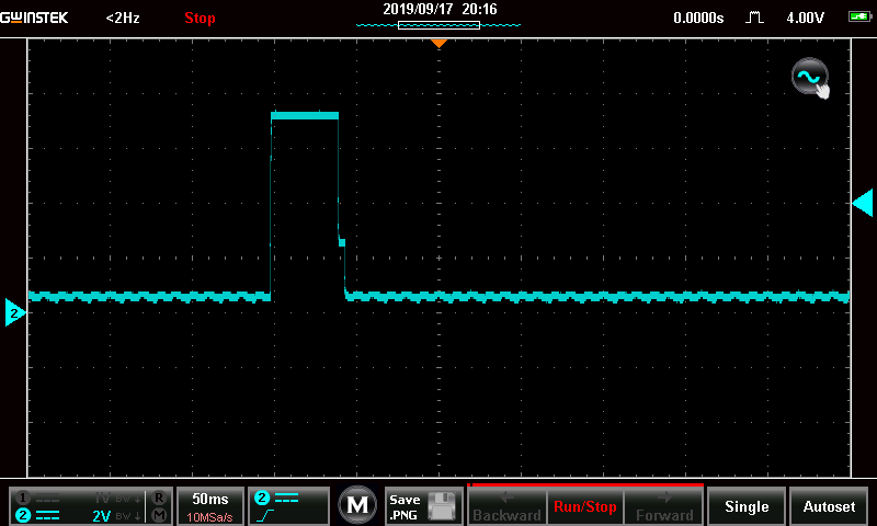
It seems like there is no response from the PD controller, but how could this happen? If this voltage is also on VDD pin, then the PD should start and do its thing?

Thank You very much for Your help!

Best Regards,

Tomas

  • Hello,

    Thank you for your question and for all of the information you included in your post. I appreciate it very much, and it helps me work faster on this. A quick glance at the schematic does not show any obvious issues. I will do a deeper dive to compare and get back to you with my findings. I will try to get to this tomorrow or Thursday. 

    For now, can you check to see what the voltage looks like on VC and VB? Thank you!

    Regards,

    Michael Pahl 

  • Hi Michael,
    thank you for your quick response. I took several measurement of different points on board.

    VDD vs VSS


    Voltage on Vc vs VSS

    Voltage Vb vs VSS

    Voltage on Vb and Vc vs GNDA (both of them were idetical, so I include only one picture)

    And just to be sure I took voltage on the inputs of the TPS23754

    Vdd vs VSS

    Vdd1 vs VSS

    I noticed that those voltages are looking pretty same, still there is no sign of ICs activity

    Best regards,
    Tomas

  • I did also test of connecting 24V adapter to see if the IC work and unfortunatly after connecting power supply, it did nothing, no voltage on the ouput. No voltage on Vc vs GNDA(RTN) or GATE vs GNDA(RTN) after some time the TPS23754 got very hot (finger cannot be placed on it) so we diconnected it. I took some measurements while doing this:

    Interesting Vc vs VSS voltage: ( which identical was on GATE pin vs VSS)


    At some point we found 15V on Vc vs GNDA (RTN) but when we tried it again it was not there anymore and it was never there after that (when we tried to repeat the process) 

    But at the same time on GATE vs GNDA(RTN) there was 0V all along. On the inputs of the TPS23754 was 22,5V. But nothing on Vc nor Vb (vs RTN).


  • Hello,

    Thank you very much for all of the scope shots. For the part getting hot, is it the whole board or just one part? Maybe a thermal image will give a clue.

    Additionally, what power level and type of load are you connecting to your design?

    Finally, I saw on another post with Darwin F. that you said you are considering a new topology. Is this the same project, or do you wish to continue debugging this board?

    Regards,

    Michael Pahl 

  • Hi,

    yes, it is the one part, which through the thermal pad heats up entire board (tried with finger). I will try to find thermal camera. For the load it is 5W 56Ohm rezistor, which should correspond for something like 2.5W on the output. The adapter is 24V,  1A.


    PS: We want to continue with this design for other application, the smaller one will be for a different one. 

    Regards,

    Tomas Nekvapil

  • Tomas,

    Thank you very much for your replies. I find it very peculiar about the gate being up so high at 22V, and the mysterious voltage on VC to RTN that came once.

    If VC = 0V to RNT then the chip is not on.I

    Can you measure from VSS to RTN? Additionally, can you power off the circuit and measure the resistance between VSS and RTN? I am trying to see if the internal pass FET is turning on / is damaged. 

    Additionally in your layout, did you connect the input earth ground to VSS or RTN? I know it is not labeled that way, but I just want to double check. 

    Regards,

    Michael Pahl 

  • Hi Michael,

    here is measurement VSS -> RTN: (measured between pins 10 and 9 respectively, measured it also between pin 1 of R5 an pin 2 of C2)

    And on the same places I measured 0.8 mega Ohms when turned off.

    I am not entirely sure, what you mean by input ground earth? Do you mean some specific pin on the chip?


    - if you are reffering to VSS - which is negative power rail derived from central taps of RJ45 connector with integrated magnetics. And this rail is connected to all Vss pins on the IC.

    Best regards,

    Tomas

  • Just adding... to further complicate the matter.

    I have just now measured the diode between VSS -> RTN and it showed 0,55V drop. Also when I measured the hotswap MOSFET resistance backwards, RTN - >VSS I got infinite(or out of range) resistance.

    So It seems like to internel MOSFET is fine.

    Tomas

  • Hello Tomas,

    Thank you again for the measurements. It is good to know the MOSFET is not damaged. 

    Going back to the post on Sept 18, where you used the 24V adapter input >> the transformer in the EVM and your schematic is not rated to run on 24V. Can you try using 48V on the adapter to see if it works?

    If it does not work in this case, I suspect there is either a damaged component or a component that is the wrong value. I would double check the values and if you are able, use the EVM as a reference. 

    Regards,

    Michael Pahl 

  • Hi Michael,

    I will test it tommorow, but beforehand I would like to ask You If You have any suggestion, which components should be checked for functionality? Personally I tried to change the detection rezistor and It did not change anything, and since it did not even passed detection I am clueless, which components could influence it. 

    Also I am quite unsure, why the reference design is using both functions APD and PPD, but with only 48V PS? I thought that PPD was mainly used for low voltage PS. Could You please recommend some that would tolerate 24V?

    Best regards,

    Tomas

  • Hello Michal,

    I tried connecting the 48V adapter and it pretty much did the same. No voltage on Vc vs RTN. Nothing on the gate of the main switching transistor. And the IC gets hot pretty quickly.

    I tried to measure voltage on Vc vs VSS (now the GND of the adapter) and it showed me 46.6V and also GNDA (RTN) vs VSS showed 46.6V both of these measurements were on the C12 transistor in the schematic is that OK? Because the GNDA vs VSS (GND of the adapter) is like that on all points on the PCB. But the Vc to RTN showed 0V.

    Best regards, 

    Tomas

  • Hi Michael,

    I would not believe it. But yet it was true. After I did all those measurements it pointed toward short between VDD - RTN. Which indeed it was. I resumed by de-soldering caps, which were fine. Then I removed the main switching transistor and I discovered a lot of tin under it. I have resoldered it and short was gone! Then I resumed by checking all the caps and resistors between connector and main IC. And I discovered that detection resistor was 470R instead of 24k9. but what suprised me the most was that in the bag which was sent to me from farnell and where should be 24k9,were all of them 470R instead. Crazy stuff. So that was it, I have put there the correct value and it WORKED!

    Thank You very much for Your support!

    Best regards,

    Tomas

  • Tomas,

    So glad you were able to find the short and some misplaced components. I's also nice to know the design was not the problem! Thank you so much for posting your findings for us. Glad we were able to support!

    Regards,

    Michael Pahl