This thread has been locked.

If you have a related question, please click the "Ask a related question" button in the top right corner. The newly created question will be automatically linked to this question.

UCD3138: External Clock Synchronization on EVM

Part Number: UCD3138

We are trying to figure out how to enable synchronization with an external clock signal on our UCD3138HSFBEVM-029 (Hard Switching Full Bridge Evaluation Module). There is a test point labeled SYNC which is connected to pin 8, ADC_EXT on the UCD3138. We are searched through the EVM user guide, ucd3138 datasheet, technical reference manual, and practical design guide, and were not able to find any information regarding the setup of an external sync clock. Can this be done with the UCD3138? If so what, if anything, needs to be reconfigured on the EVM to accept a sync input?


  • Hello Scott,

    Pin #8 which is set by default as ADC_EXT_TRIG, but it can also be configured as TCAP, SYNC or PWM0 using the IOMUX register.

    Configuring pin #8 as SYNC is not what you need. SYNC is a way to synchronize between the PWM output waveforms from two or more UCD3138s.

    What is the purpose of "External Clock Synchronization" in your application? Do you look for better clock frequency accuracy?

    If so, you would need to configure pin #8 as TCAP (timer capture pin) and use the code from the attached application note to adjust the internal timings based on the external clock reference.

    Regards,

    Compensating for oscilator frequency variations in UC3138.docx

  • Thank you for your response.

    It is being driven by an upper level requirement. It can not be free-running, and needs to synchronize to a RS-422 signal. Can this be achieved with pin #8 configured as SYNC, or possibly by utilizing TCAP in another way than described in the document you provided?

  • Depending on the baud rate, it can probably sync to an RS-422.

    But since RS-422 has different high or low pulse widths (based on consequent number of bits at 1 or 0), the firmware need to change and will be more complex.

    Regards,

  • The sync signal will be provided via RS-422 but can be translated before input to the UCD3138. Is it possible to synchronize the switching frequency with an external signal? If so what configuration of pin #8 is needed?

  • Adjusting the switching frequency as a one time deal is no problem.

    But adjusting the switching frequency on the fly and periodically, specially when the frequency of the external signal can vary significantly, can be challenging.

    In any case, this is not handled entirely by hardware, and some firmware will be required.

    Does the RS-422 serve as a real communication channel or it will solely provide a periodic clock signal for the purpose of synchronization?

    The first case is a little bit harder to implement, but it is doable. The second case requires less firmware.

    As in the application note that I have sent you pin #8 should be configured as TCAP, By:

    MiscAnalogRegs.IOMUX.bit.EXT_TRIG__MUX_SEL = 1;

    Then based of the time value read from the timer capture the firmware needs to adjust the period of the DPWMs.

    Hope this helps, but if the above is not specific enough for you, then we need to discuss your application in details first.

    Regards,

  • Please also note, if the external signal carries the same frequency as the switching frequency, then there might be alternative routes to handle this. Please advise.

  • The RS-422 is not being used as a real communication channel. We intend to convert the signal back to a single ended 3.3V signal and would like to synchronize the switching cycles to this signal.

    The sync signal will be 400kHz +/- 5kHz. We want the switching cycle of the converter to be synchronized with this signal. Usually we expect a free running frequency to be set below the intended sync frequency to allow the converter to continue to run without the presence of the sync frequency.

    I do not see how measuring time values with the timer capture will help. I would think we would need to synchronize one of the DPWMs to this external sync signal in order to synchronize the switching cycle.

  • Not only do we want the switching frequency to be the same as this external signal, but we also want the two synchronized.

  • OK, things getting clear now.

    So you are not referring to external clock, but synchronization between PWMs.

    In that case you do need to configure pin #8 as SYNC ( MiscAnalogRegs.IOMUX.bit.EXT_TRIG_MUX_SEL = 2;)

    A positive edge on SYNC pin resets the DPWM counter in UCD3138, therefore both the frequency and the phase stay fixed compare to the external signal.

    The only issue with this is that if Event4 is configured before the end of period, and if the external frequency is substantially higher than the DPWM frequency, then this resetting of the DPWM can happen before Event4 and can cause pulse extension. For this reason, we would recommend that you configure Event4 as zero.

    Hope this makes sense

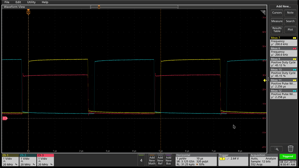
  • Referencing this post https://e2e.ti.com/support/power-management/f/196/t/298579?unable-to-get-UCD3138-external-sync-working we were able to get external sync partially working. DPWM0 is synced to the external signal although the phase delay changes with frequency. We are testing with the J2 jumpers removed so we can examine the gate signals without cycling the fets. With the external signal frequency = hard coded frequency, the DPWMs behave as expected with duty cycle = 45%. (Ch1: DPWM0A, Ch2: DPWM1A, Ch3: External Sync Signal)

    If our sync frequency increases, the rising edge of DPWM1 remains at 1/2 the hard coded period, but the pulse width reduces as DPWM0's pulse width remains the same.

    If our sync frequency goes lower than the hard coded frequency, DPWM1's pulse width remains the same while DPWM0 pulse width increases and pushes the rising edge of DPWM1 >1/2 hard coded period.

    Could you please review our code to see if we are on the right track?

    void init_dpwm0(void) // DPWM0B is Used to drive Sync-FET
    {
    Dpwm0Regs.DPWMEV1.all = 540; // deadtime_CD;
    Dpwm0Regs.DPWMEV3.all = (pmbus_dcdc_config[0].period >> 1); // (period >> 1) + 0; // deadtime_EF; // Modified for Single_Frame 
    Dpwm0Regs.DPWMCTRL0.bit.PWM_MODE = 0; // Set to normal mode 
    Dpwm0Regs.DPWMCTRL0.bit.CLA_EN = 1;
    #ifdef CYCLE_BY_CYCLE_CURRENT_LIMIT
    Dpwm0Regs.DPWMCTRL0.bit.CBC_PWM_AB_EN = 1;
    #endif
    Dpwm0Regs.DPWMCTRL1.bit.GLOBAL_PERIOD_EN = 1;
    Dpwm0Regs.DPWMCTRL1.bit.EVENT_UP_SEL = 1; // Events update at the end of period
    Dpwm0Regs.DPWMCTRL1.bit.CHECK_OVERRIDE = 1; // Normally CLA == 0 is considered a fault; Set the check-override so cla==0 is valid
    Dpwm0Regs.DPWMCTRL1.bit.ALL_PHASE_CLK_ENA = 1; // Need all phases for hi Resolution
    Dpwm0Regs.DPWMCTRL2.bit.SAMPLE_TRIG_1_EN = 1;
    Dpwm0Regs.DPWMCTRL0.bit.PWM_EN = 1;
    Dpwm0Regs.DPWMSAMPTRIG1.all = (pmbus_dcdc_config[0].period)- 6240; //2100; 279*16ns = 4.464us;-5000; // Writing to all in order to normalize to high resolution
    Dpwm0Regs.DPWMCTRL1.bit.GPIO_A_EN = 0;
    Dpwm0Regs.DPWMCTRL1.bit.GPIO_B_EN = 0;
    Dpwm0Regs.DPWMCTRL1.bit.SYNC_FET_EN =0;
    // Dpwm0Regs.DPWMPHASETRIG.all = (period)>>1;
    //*******************************************************
    //this is only for unbalancing current without blocking cap
    Dpwm0Regs.DPWMCYCADJA.all = 0;
    //******************************************************
    Dpwm0Regs.DPWMCTRL0.bit.MSYNC_SLAVE_EN =0; // DPWm0 is master
    MiscAnalogRegs.GLBIOEN.bit.ADC_EXT_TRIG_IO_EN = 0;//SPECIAL FUNCTION // SRS 10/4/19 code added
    MiscAnalogRegs.IOMUX.bit.SYNC_MUX_SEL = 2; // // SRS 10/4/19 code added
    MiscAnalogRegs.IOMUX.bit.JTAG_CLK_MUX_SEL = 0; //default is 2 // SRS 10/4/19 code added
    MiscAnalogRegs.IOMUX.bit.EXT_TRIG_MUX_SEL = 2; //SYNC // SRS 10/4/19 code added
    LoopMuxRegs.SYNCCTRL.bit.SYNC_DIR = 1; // SRS 10/4/19 code added
    }


    void init_dpwm1(void) // DPWM1B is Used to drive Sync-FET

    Dpwm1Regs.DPWMEV1.all = 540; //deadtime_GH; //(period >> 1) + deadtime_GH;
    Dpwm1Regs.DPWMEV3.all = (pmbus_dcdc_config[0].period >> 1); // + deadtime_AB; // Modified for Single_Frame
    Dpwm1Regs.DPWMCNTPRE.all = pmbus_dcdc_config[0].period >> 1; // Shift by 180 degree ( half the period)
    Dpwm1Regs.DPWMCTRL0.bit.PWM_MODE = 0; // Set to normal mode 
    Dpwm1Regs.DPWMCTRL0.bit.CLA_EN = 1;
    #ifdef CYCLE_BY_CYCLE_CURRENT_LIMIT
    Dpwm1Regs.DPWMCTRL0.bit.CBC_PWM_AB_EN = 1;
    #endif
    Dpwm1Regs.DPWMCTRL1.bit.GLOBAL_PERIOD_EN = 1;
    Dpwm1Regs.DPWMCTRL1.bit.EVENT_UP_SEL = 1; // Events update at the end of period
    Dpwm1Regs.DPWMCTRL1.bit.PRESET_EN = 1; // Preset enabled
    Dpwm1Regs.DPWMCTRL1.bit.ALL_PHASE_CLK_ENA = 1; // Need all phases for hi Resolution
    Dpwm1Regs.DPWMCTRL1.bit.CHECK_OVERRIDE = 1; // You have to set this bit if E4 is set less than E3
    Dpwm1Regs.DPWMCTRL1.bit.GPIO_A_EN =0;
    Dpwm1Regs.DPWMCTRL1.bit.GPIO_B_EN =0;
    Dpwm1Regs.DPWMCTRL0.bit.PWM_EN = 1;
    Dpwm1Regs.DPWMSAMPTRIG1.all = 2000; // sample trigger for FE2 to sample input voltage
    Dpwm1Regs.DPWMCTRL0.bit.MSYNC_SLAVE_EN =1; // DPWm0 is master, DPWM1 is slave
    Dpwm1Regs.DPWMCTRL1.bit.SYNC_FET_EN =0;
    }


    void init_dpwms(void)
    {
    LoopMuxRegs.PWMGLBPER.all = pmbus_dcdc_config[0].period;
    init_dpwm0();
    init_dpwm1();
    configure_dpwm_timing();
    MiscAnalogRegs.GLBIOEN.all |= 0xFF; //set to globe gpio mode
    MiscAnalogRegs.GLBIOOE.all |= 0xFF; //set to output mode
    MiscAnalogRegs.GLBIOVAL.all &=0xFFFFFF00; //output 0 at GPO mode
    LoopMuxRegs.GLBEN.all|= 0x0F;//Enable all DPWMs
    Dpwm0Regs.DPWMCTRL1.bit.EXT_SYNC_EN = 1; // SRS 10/7/19
    Dpwm1Regs.DPWMCTRL1.bit.EXT_SYNC_EN = 1; // SRS 10/7/19
    LoopMuxRegs.DPWMMUX.bit.DPWM0_SYNC_SEL =0; //DPWm0 is a master
    LoopMuxRegs.DPWMMUX.bit.DPWM1_SYNC_SEL =0;//DPWm1 is a slave, syc with DPWM0
    LoopMuxRegs.DPWMMUX.bit.DPWM2_SYNC_SEL =0;//DPWm2 is a slave, syc with DPWM0
    LoopMuxRegs.DPWMMUX.bit.DPWM3_SYNC_SEL =0;//DPWm3 is a slave, syc with DPWM0
    }

    Period is still based on the hard coded value so we may need to implement some timing adjustments as outlined in the document you attached in your initial response. We are just unsure if there is a better configuration which would avoid this issue altogether. Thank you for your help thus far.

  • Your response makes sense except for the line of code you provided.

    As I understand the Technical Reference Manual SNIU028A, (MiscAnalogRegs.IOMUX.bit.SYNC_MUX_SEL = 0;) would configure the I/O pin "SYNC" to keep it's primary assignment, "DPWM Synchronize pin". 

    But the 40 pin UCD3138 does not have an I/O pin "SYNC". Pin #8 is ACD_EXT_TRIG with the primary assignment of "ADC conversion external trigger input".

    Instead it makes sense for me to configure I/O pin "ADC_EXT_TRIG" (pin #8) with the alternate assignment "SYNC" using (MiscAnalogRegs.IOMUX.bit.EXT_TRIG_MUX_SEL = 2;). This is what I did in the code shown in my previous response. 

    I would like verification that I understanding the Technical Reference Manual because your suggested code does not make sense to me.

  • You are right.

    MiscAnalogRegs.IOMUX.bit.EXT_TRIG_MUX_SEL = 2; is what you need to set pin #8 as SYNC.

    Furthermore, you could still connect the timer capture capability to pin #8 by setting the CAP_SEL bitfield to 3. 


    This way not only the SYNC mechanism works. But also the timer capture can measure the period to adjust the period of the slave if required.

    Regards,

  • Unfortunately there is no hardware configuration that takes care of all cases.

    What is your topology? What your Event4 is set to?

    Some firmware help may be required.

    Regards,

  • It is a hard switching full bridge. Currently there are only minimal mods to the stock EVM firmware. DPWM0 and DPWM1 use output B for synchronous rectification. I am not sure how the stock firmware handles EV4 just yet. I will need to look into that more. 

    I am also tying to figure out how to setup timer capture...

    Thank you for your continual help.

  • According to the best of my knowledge the HSFB EVM code does not set the Even4 to zero.

    Therefore the chance of pulse extension when SYNC is used needs to be considered.

    Regards,

  • Hi Scott,

    Have you had the chance to figure out timer capture?

    Do you need any help in setting Event4 to zero and still maintaining the same dead times?

    Regards,

  • I have pin #8 set to SYNC and CAP_SEL set to SYNC which seems to be working properly. Based on the document you provided about internal frequency 
    compensation, I attempted to calculate compensation for my external signal variation. This compensation will be used to adjust the switching period as
    defined by the HSFB EVM firmware. In the standard interrupt I start by calculating the difference between the current value of CAP_DAT and the previous value
    of CAP_DAT, but my result leads me to believe the standard interrupt occurs every 1.15ms. Most documentation states the standard interrupt occurs every
    100us while the document you provided in your first post also references 91.553us. When I look at t24_latched_diff via UART it is equal to 17,960 +/-5. When I
    look directly at CAP_DAT via UART I confirmed it increments by about 17,960 each time the standard interrupt occurs.
    17,960 * 64ns = 1.15ms
    I don't understand what is wrong here.
    	MiscAnalogRegs.IOMUX.bit.SYNC_MUX_SEL = 2; //config SYNC pin as Ext Trig 		// SRS 10/4/19 code added (defaults is 0 (SYNC), 40p device doesn't have this pin)
    	MiscAnalogRegs.IOMUX.bit.JTAG_CLK_MUX_SEL = 0; //config CLK pin as CLK			// SRS 10/10/19 (default is 2 (SYNC))
    	MiscAnalogRegs.IOMUX.bit.EXT_TRIG_MUX_SEL = 2; //config EXT TRIG pin as SYNC	// SRS 10/4/19 code added (configure pin 8 as SYNC)
    	TimerRegs.T24CAPCTRL.bit.CAP_SEL = 3;											// SRS 10/11/19 timer capture pin select configured for SYNC pin
    	TimerRegs.T24CAPCTRL.bit.EDGE = 1;												// SRS 10/11/19 capture the 24 bit timer value on a rising edge of SYNC signal

    Above is from my initdpwm0 and below is in the standard interrupt.


    if(TimerRegs.T24CAPCTRL.bit.CAP_INT_FLAG)
    	{
    		t24_latched = TimerRegs.T24CAPDAT.bit.CAP_DAT; 			// read capture data register
    //		v = TimerRegs.T24CAPDAT.bit.CAP_DAT;
    
    		if(t24_latched > t24_latched_previous)				// if no overflow
    		{
    			t24_latched_diff = t24_latched - t24_latched_previous;
    		}
    		else													// if overflow
    		{
    			t24_latched_diff = t24_latched + 0xFFFFFF - t24_latched_previous;
    			char_out(222);
    		}
    
    		v = t24_latched_diff;
    		a[0] = v >> 24;
    		a[1] = v >> 16;
    		a[2] = v >>  8;
    		a[3] = v;
    		char_out(a[0]);
    		char_out(a[1]);
    		char_out(a[2]);
    		char_out(a[3]);
    		t24_latched_previous = t24_latched;

  • I have not yet looked into Event4 as I am focused on period compensation for the variation in external sync signal. Below is read from a terminal while i was writing CAP_DAT

    0 63 65 231 0 63 136 17 0 63 206 59 0 64 20 25 0 64 90 70 0 64 160 110 0 64 230
    154 0 65 44 200 0 65 114 242 0 65 185 30 0 65 255 73 0 66 69 116 0 66 139 81 0 6
    6 209 123 0 67 23 167 0 67 93 212 0 67 163 255 0 67 234 41 0 68 48 83 0 68 118 1
    27 0 68 188 170 0 69 2 134 0 69 72 176 0 69 142 216 0 69 213 2 0 70 26 220 0 70
    97 7 0 70 167 48 0 70 237 89 0 71 51 128 0 71 121 168 0 71 191 209 0 72 5 250 0
    72 76 36 0 72 146 79 0 72 216 123 0 73 30 92 0 73 100 139 0 73 170 184 0 73 183
    72

    I thought TimerRegs.T24CNTCTRL.bit.PRESCALE might be set but i looked in the memory debugger and it was 0.

  • I am now unsure If it is working as expected. Even if standard interrupt was occurring every 1.15ms i would expect t24_latched_diff to have an inversely proportional relationship with the frequency of my external sync signal. I tried adjusting this sync signal in intervals of 1kHz, 100Hz and 10Hz. Regardless, t24_latched_diff bounces around near 17,955 +/- 5 with some outliers. I expect some drift based on internal frequency but something is not right here.

  • Setting Event4 to zero is an easier task than making TCAP work. And it might be all you need.

    If the EVM code Event4 is set before the end of period, and the dead time is equal to ((Period -EV4)+ Ev1)

    If you set EV4=0, then the dead time is equal to (Ev1 -Ev4 =Ev1)

    So if you set EV4 to zero, you need to set EV1 to a larger value (Add the original (Period -EV4) value to EV1).

    The reason for setting EV4 to zero is that it will prevent pulse extension.

    This is due to the fact that after any reset of the DPWM counter, the value of B output will be forced to go low.

    Hope this makes sense.

    Regards,

  • For initial testing i commented out the original Event 4 lines of code and set it to 0. I then added pmbus_dcdc_config[0].deadtime_X to Event 1 in each module. Regardless, Event 2 is calculated from a period that does not vary with the external sync signal. That is why i thought i needed compensation. With EV4 = 0 it appears to occur sooner when viewing on an oscilloscope, leaving more deadtime between syncFET signals.

    void configure_dpwm_timing(void)
    {
      	Dpwm0Regs.DPWMEV2.bit.EVENT2 = (pmbus_dcdc_config[0].period >> 1) 
      	                               - pmbus_dcdc_config[0].dead_time_2;													  
    /*
        Dpwm0Regs.DPWMEV4.bit.EVENT4 = (pmbus_dcdc_config[0].period
                                       - pmbus_dcdc_config[0].dead_time_1) + 540;
    
      	if(Dpwm0Regs.DPWMEV4.bit.EVENT4 > pmbus_dcdc_config[0].period )
      		Dpwm0Regs.DPWMEV4.bit.EVENT4 = Dpwm0Regs.DPWMEV4.bit.EVENT4 - pmbus_dcdc_config[0].period;
      	else
      		Dpwm0Regs.DPWMEV4.bit.EVENT4 = Dpwm0Regs.DPWMEV4.bit.EVENT4;
    */
      	Dpwm0Regs.DPWMEV4.bit.EVENT4 = 0;					// SRS 10/15/19 to prevent pulse extension
      	//////////////////////////////////////////////////////////////////
      	Dpwm1Regs.DPWMEV2.bit.EVENT2 = (pmbus_dcdc_config[0].period >> 1) 
      	                               - pmbus_dcdc_config[0].dead_time_4;
    /*
        Dpwm1Regs.DPWMEV4.bit.EVENT4 = (pmbus_dcdc_config[0].period 
                                       - pmbus_dcdc_config[0].dead_time_3) + 540;
    
      	if(Dpwm1Regs.DPWMEV4.bit.EVENT4 > pmbus_dcdc_config[0].period )
      		Dpwm1Regs.DPWMEV4.bit.EVENT4 = Dpwm1Regs.DPWMEV4.bit.EVENT4 - pmbus_dcdc_config[0].period;
      	else
      		Dpwm1Regs.DPWMEV4.bit.EVENT4 = Dpwm1Regs.DPWMEV4.bit.EVENT4;
    */
      	Dpwm1Regs.DPWMEV4.bit.EVENT4 = 0;					// SRS 10/15/19 to prevent pulse extension
    }

  • Sorry for updating this post with related issues. It has grown substantially. DPWM0 is currently synchronized with my external signal which was the main purpose of the original post. Thank you for your help. I do have outstanding issues with TCAP, but I will start a new post for clarity.