This thread has been locked.

If you have a related question, please click the "Ask a related question" button in the top right corner. The newly created question will be automatically linked to this question.

LMG1205: Power management forum

Part Number: LMG1205

Hey Everyone,

I am currently working on a Bldc Driver of 1 kW using GaN device and LMG1205,while on it i have faced certain problem hope you can help me solve this issue.

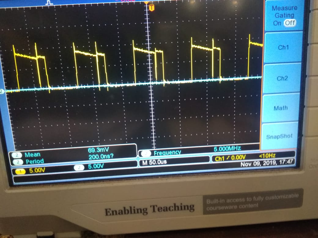
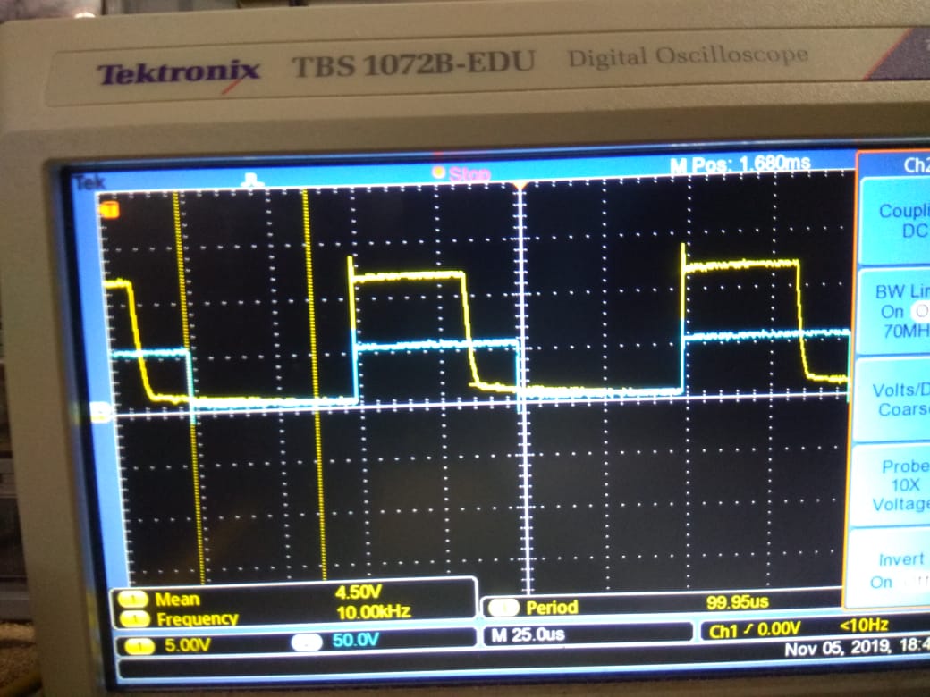
1.The input voltage i.e Vds=12v,Vdd = 5v,load resistance on a single phase 570 ohms ,input frequency 10kHz @50% duty.As expected the HOH/HOL should also turnon and turned off at same input frequency but the gate(HOH/HOL) is getting turned off before only at 38%,Why? (For you reference i have attached waveform below) .

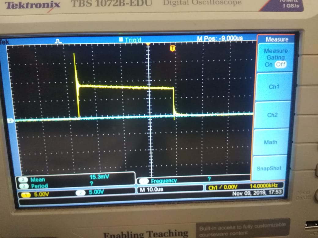
2.Also the LMG1205 is showing unexpected outcome below 10 kHz frequency?The ringing in the image shown Below is in the 50% of the duty i.e. rest half is always low.   

FYI Bootstrap capacitor is 0.1uf .

Thanks and Regards.


  • Hi Rahul, 

    Thanks for reaching out about lmg1205 sorry to hear about this issue.

    Can you share the 1205 and FET portion of the schematic? 

    For P1, what is the blue waveform? At 50v?

    Can you take a scope shot of 1205 HI, LI, HO, LO with respect to VSS?

    Also can you make sure the VDD and HB-HS cap supply is at 5v during operation and not dipping below UVLO?

    What application is this? How come the switching frequency is so low while using GaN?

    Thanks,

  • Hey Jeff,

    Thank for look into this,

    Attached below is the schematic that we are working on.

    DRIVER_1.0.pdf

    For P1,the Blue waveform is the input to HI and it is actually 5V but zoomed 10x times and also the LI pin is grounded/Vss.

    Sorry ,actually i forgot to attach the image of gate pulse but here it is .(Yellow -> HS & Blue -> HO/Gate at high side) Lo is always 0v when measured.

    Yes,we have make sure that the VDD supply is always 5V and and HB-HS cap the voltage is around 4V,which i guess is correct enough.

    I totally agree with you that the frequency is quite low ,when we talk about GaN device because its capability is much higher but currently since we are in test phase so,we decided to check at a lower frequency and then go for higher one.Moreover ,we are working on Bldc Drive and this a BLDC driver of 3 Phase.

    Hope ,this will help.

    Thanks and Regards

    Rahul  

  • Hi Rahul,

    thanks for the update,

    HO-HS gate voltage waveform looks to be 3V (at a 5V/div range). It looks like the HB-HS cap is not remaining charged for this low frequency operation, typically for low frequency switching a floating supply is needed to keep the HB-HS cap charged. If the lowisde FET pulls the switch node to ground during the HO offtime the HB-HS cap can charge back up through the internal 1205 boot diode. However if there is no LO signal to bring the switch node to ground to charge the bootstrap its possible the driver is reaching UVLO and the load is RC discharging the switch node.

    Can you share a scope shot with HO, LO, HS and HB - HS?

    This should allow us to see if HO and LO are complementary so the bootstrap charging can take place as well as monitor the high side drive voltage to make sure this stays above the UVLO voltage of about 3.2V.

    The gate waveform looks increasingly ringy, can you share your layout to make sure we have the optimal placement and routing?

    Does the issue change with no load? heavy load?

    whats your target max switching frequency?

    Thanks,

  • Hey Jeff ,

    Correct me if i am wrong ,as you said

    " It looks like the HB-HS cap is not remaining charged for this low frequency operation, typically for low frequency switching a floating supply is needed to keep the HB-HS cap charged. If the lowisde FET pulls the switch node to ground during the HO offtime the HB-HS cap can charge back up through the internal 1205 boot diode. However if there is no LO signal to bring the switch node to ground to charge the bootstrap its possible the driver is reaching UVLO and the load is RC discharging the switch node."

    But don't you think if the output i.e. HS is connected to ground through 570 ohms resistance then at any period of time (even in HO offtime),then how can a Hs be floating at any period of instance.

    Give me a day time to get  scope shot with HO, LO, HS and HB - HS.

    Below is the image of one of the phase of our layout.

    Yes,this change with the increase in the load ,the voltage drops down.

    Currently our target of running BLDC motor is at 20kHz ,gradually we would like to increase it up to 100 kHz accordingly. 

    Thanks and Regards

    Rahul

  • Hi Rahul,

    Thanks for the update, The bootstrap may not be getting a change to fully replenish itself due to the large 500ohm resistor in the charging path. Is it possible for this resistor to be under 50ohms or will there be too much power loss? are you able to switch on the Lowside if only for nanoseconds to replenish the bootstrap?

    When HO turns on the voltage on the switch node goes high so the high side driver needs to be with respect to the switch node to drive the gate from the source which makes it floating with respect to the 0V hard ground.

    The 100khz motor high frequency is to reduce motor torque ripple for better efficiency? as well as reduce the magnetics/size?

    See the attached layout review, please let me know if you have any questions. e2e layout review 100khz GaN motor.pdf

    Thanks,

  • Hey Jeff,

    Taking your suggestion we conducted a new test at 10 ohms of load  and this time we also reduced the drain to source voltage to 5v.

    Thought this time we have started getting the output gate of 50% duty but  still there are various doubts.The image are attached below:-

    This the HS->Vss as well HO->Vss plot when frequency is 11kHz and Rload 10 ohms.

    This the HS->Vss as well HO->Vss plot when frequency is 12kHz and Rload 10 ohms.

    This the HS->Vss as well HO->Vss plot when frequency is 13kHz and Rload 10 ohms

    This the HS->Vss as well HO->Vss plot when frequency is 14kHz and Rload 10 ohms.

    We are not getting this behavior as the capacitor charging is also quite low as compared to pulse gien for charging then why is it getting discharged and moreover once it is discharged how in b/w pulse it is getting charged ,this we are not getting totally.if you can help us here ,it will be great.

    Moreover Regarding your suggestions for the layout :-

     1.Regarding the gate resistor ,i understood it and will reduce it.

    2.Regarding  HS connection this is just the top layer which is visible to you we have a kept complete plain on bottom layer,the via on the via on cap are kept for that reason only.

    3. Regarding Through hole ,these are just temporary testing purpose pin when our all testing is done ,still if you can suggest to improve it we will surely like to do it.

    Thanks and Regards

    Rahul   

  • Hi Rahul,

    Sounds good thanks for the update, since changing the load does not make things worse its likely your layout is very good and is probably not causing an issue.

    It appears this issue is frequency dependent and we know the HB-HS voltage is not getting recharged and dipping below UVLO. We tried to supply a better bootstrap charging path but the turn on time if so long that it the load on the switch node is draining the HB-HS cap more than it can charge. My suggestion is to keep the load at 500 ohms but add more HB-HS cap to support the longer on times. Since HB-HS increases the rule of thumb is VDD cap should also increase by 10. Please try the same test after adding an additional 470nF or 1uF cap to HB-HS and 1uF - 10uF to VDD (keeping the 10x rule of thumb). Please let me know if you have any questions about this possible solution to the issue and Please let me know if this helps the issue.

    Thanks,

  • Hey Jeff,

    Sorry for the delay,

    But if i am not wrong then DATASHEET of LMG1205 clearly states a formula to calculate the capacitance of HB-HS cap and if I go with it then 0.1uf is absolutely correct ,then can help me in understanding why this higher value of capacitor is needed.

    Thanks,

    Rahul

  • Hi Rahul,

    Thanks for the update,

    It seems the reason why we need extra capacitance is because there is a load or resistor to ground on the switch node which is draining the charge from this capacitance during on time.

    Either we can find a way to replenish the bootstrap more often or find a way to replenish even more by increasing the capacitance enough to keep the switch high side FET on during the entire on time.

    Please let me know if you have any more questions.

    Thanks,

  • Hey,

    Then how to do we calculate the minimum load/resistance for a particular capacitance let's say 0.1 uf because in our case the the charging time was much higher than the theoritical calculated charging time,but it didn't worked.

    Thanks in advance

    Rahul.

  • Hi Rahul,

    Any additional load on HS will deplete the HB-HS cap with respect to the RC time constant during HO on time. When HO turns on it charges the HO gate however since there is a load on HS there is leakage from the HB-HS cap to ground. The amount of capacitance that is required depends on this amount of leakage as well as the duty cycle that the leakage happens during. How much additional charge is removed from the bootstrap cap during HO on time? since Q=C*V then the minimum additional capacitance required to counteract the leakage is Q/5V.

    Check out the app note below for help with this bootstrap cap calculation. Let me know if you have any questions on this.

    Thanks,