This thread has been locked.

If you have a related question, please click the "Ask a related question" button in the top right corner. The newly created question will be automatically linked to this question.

UCC28951-Q1: Abnormal PWM Wave during soft starter that make my tool short-cirtcuited UCC28951

Part Number: UCC28951-Q1
Other Parts Discussed in Thread: UCC28951, UCC27714

Hello, i have several problem during my final assignment using UCC28951 to make battery charger of electric vehicle.

Vinput should be 220Vac and Voutput should be 60 Vdc (my battery nominal rate is 48V ; 12V accumulator x 4)

When i give 100Vac below, everything look normal. No noise in transformer, MOSFET (using 6R190C6) temperature max 30 degree celcius, and i can give load up to 5A using electronic DC load.

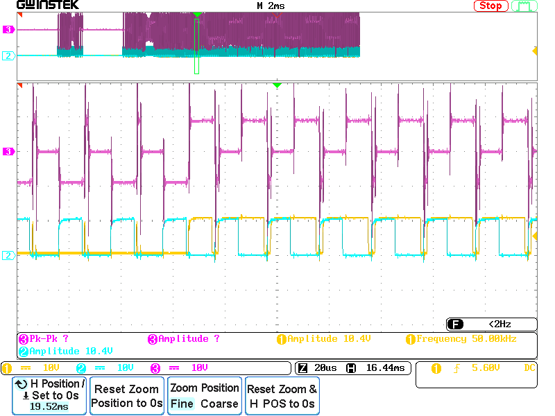
When i increase the input voltage, which is 150Vac, the fuse on the input side blown up and my MOSFET (right leg, upper side and lower side) broken. I analyze the problem using oscilloscope after i replace the broken MOSFET. Here is the picture of the wave.

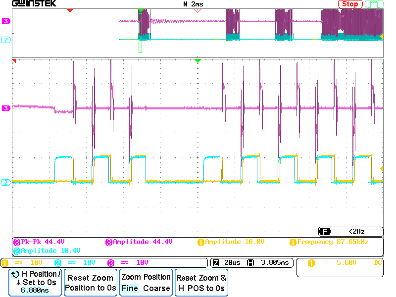
(yellow: OUTB, blue: OUTD, purple: transformer output)

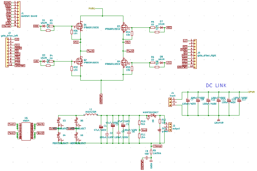
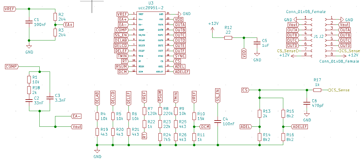
this wave was supplied by 30Vac, which converted to dc by multiplying with 1.414. I guess i have no problem with soft starting as it only place capacitor. Here is the schematic:

Please let me know where is my mistake, as i want to finish it to my final project.

  • Hello Hanif

    Attached is a general purpose debug procedure you can follow to identify the cause of the problem although you seem to have been able to make some good progress already./cfs-file/__key/communityserver-discussions-components-files/196/6177.UCC28950_2C00_-UCC28951-Debug.docx

    Looking at the waveforms you posted you can see that the OUTB waveform is ok. The first OUTD waveform in the burst of pulses is occasionally shorter than usual - this behaviour is expected and is noted in the data sheet under Figure 1. This won't cause problems if you are using gate driver transformers but if you are using a high side driver IC (UCC27714 or similar) you must be careful with the layout to make sure that the narrow pulse can charge the bootstrap capacitor sufficiently. 

    Having said that, I don't think that the driver circuits are the problem. There is a lot of ringing, or high voltage spikes on the transformer waveform. This tells me that there is a lot of unclamped inductive energy in the transformer circuit - perhaps long traces from the transformer to the rectifiers or long traces on the transformer primary circuit. The transformer leakage inductance can also cause these spikes.

    You should review the secondary snubber circuits and their layout. Spikes like this have a lot of high frequency energy so the snubber circuit must be laid out carefully so that it is effective at these frequencies.

    I'd suggest that you disable the SRs by disconnecting their gate drivers and connecting their gates to their sources. The SRs will then behave as diodes.

    You can use TVS (Transient Votlage Suppression) diodes, sometimes called Transils, to clamp the spikes so that the SRs (Diodes) do not avalanche. This should prevent them from failing while you investigate the root cause of the problem.

    Please post a copy of your PCB layout here - Gerber files or the original files along with the full schematic and I can review it to see if there are any areas that can be improved.

    Regards
    Colin

  • Thanks for the reply.

    I've reviewed the Figure 1 in datasheet, and OUTB with OUTD seem like they are in one phase correctly. But the problem is about the waveform of OUTD lil bit shorter than usual right? From the controller section, how could it happen? 

    Also i have some pictures to take attention on it, because it looks so strange. This is the picture:

    The start up process begun again in the middle of the waveform, not only at the beginning since the controller is turned on. Could you give me an explanation about that? Thanks.

    Here is my PCB layout also with the schematic. I put the kiCAD file so thus you can inspect more. Thanks Colin.

  • Sorry for the PCB file isn't attached yet.

    0385.PCB.rar

  • I forgot to tell you that i dont use SRs, i use Fullbridge rectifier diode on my secondary side after transformer. Thanks.

  • Hello Hanif

    The Current Sensing is located in the wrong place, it should be sensing the input current to the bridge not the output current. The system is giving you alternate Dmax and Dmin pulses - almost certainly because of the incorrect current sensing.

    Regards
    Colin

  • I'm sorry, that was my old current sensing method. I'm not using R-shunt anymore, and using TA12-100.

  • Hello Hanif

    That's ok, the current sensing method does not matter as much as the current sensing location. The current must be sensed at the input to the bridge.

    Please let me know how you want the output to behave if there is an overload ? Is a simple current limit which is relatively inaccurate ok or do you need an accurate CI/CV characteristic like that needed for battery chargers.

    Regards

    Colin

  • Hello Colin,

    Actually for this stage, i just want my converter works as safe as it can, like the MOSFET isn't getting hotter, no hissing in transformer and induktor, so i can take another step to designing battery charger.

    And also i'm little bit worrying about the COMP pin, the component is only resistor and capacitor get parallel together, how significant it will affect if i change those numbers?

    Thanks.

  • Hello Hanif

    The compensation network, C2, C3, R1, R18 is correct although you may need to adjust the values.

    There is a lot of material available about control loops online and here are some links to Switched Mode Power Supply control loops. I think your should play the training video first because it is a basic introduction to stabilising control loops.

    http://www.ti.com/lit/ml/slup098/slup098.pdf 

    https://www.ti.com/seclit/ml/slup113/slup113.pdf

    https://training.ti.com/control-smps-refresher?keyMatch=REFRESHER&tisearch=Search-EN-everything

    One thing you could try is to run the power stage open loop - tie EA- to 0V so that the controller runs at Dmax all the time. Increase the DC link voltage slowly from 0V until the output reaches 60V and then stop. You will be able to confirm that the power stage is switching cleanly.

    I will need to see your full schematic before I can offer much  more advice. Please let me know how you get on.

    Regards

    Colin

  • Hi Hanif,

    I has been over a week since TI's last response on this post and I hope you have made progress on this issue. I am going to close this post. Please open a new post if you have more questions.

    Regards

    Peter