This thread has been locked.

If you have a related question, please click the "Ask a related question" button in the top right corner. The newly created question will be automatically linked to this question.

TPS82130: Propagation delay of PG outpu

Part Number: TPS82130

Hi

My customer has question.

The following is described in the explanation of the PG output of TPS82130.
However, when the waveform is confirmed, PG falls to Low after the input voltage rises to about 1.6V.

The PG pull-up destination is the input voltage.

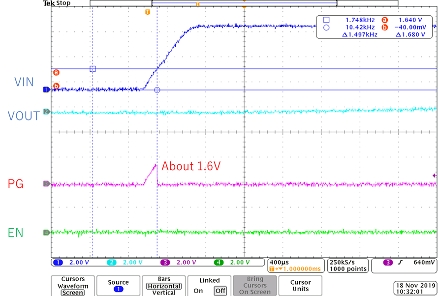
Probably there is a delay time, is this behavior correct?
If there is a delay time, how long is it?

Best Regard

T Kishi

  • Hi T,

    PG is a power good output pin. It will only pull high once the output is regulated. From the looks of the waveform EN never pulls high and VOUT is at 0V. The PG pin momentarily is pulled high because it is connected to VIN but then sharply goes low because the part is not enable and regulating.

    To truly exercise the PG pin you should pull EN pin high so that the device starts to regulate. The delta in VIN applied to PG pin  being pulled high will be the delay time. 

    Regards,

    Jimmy

  • Hi Jimmy

    Thank you for reply.

    The datasheet states PG = Low when 0.7V <VIN <VUVLO.
    In other words, the PG pin can only be expected to rise to about 0.7V.
    However, when checking the waveform, it has risen to about 1.6V.
    This is too wide for an error range of 0.7V. (Approximately 2.2 times)
    It is expected that there will be a delay time until VIN exceeds 0.7V and the PG output is confirmed. Is this idea wrong?

    Best Regard

    T Kishi

  • Hi T Kishi,

    Thank you for the clarification. I understand the problem now.

    Your thought is correct that the PG pin should have been low around 0.7V instead of 1.6V that you see in your waveform following Table 1 of the datasheet. 

    I have a few suggestions below:

    1. This time delay is not specified in the datasheet so I will have to track the apps engineer who previously worked on this device. Additionally I will order an EVM to test in the lab and confirm delay. However I would suggest you test the following to understand the delay. If possible can you slowly ramp VIN in 100mV increments and monitor when the PG pulls high? Perhaps the PG signal will pull low earlier than 1.6V if the input voltage ramps slowly and the device is able to respond. The delta between VIN reaching 0.7V and PG logic status low will be your time delay. 
    2. Also can you provide the schematic to your customer's circuit? From the waveform, it looks like PGOOD is tied to VIN through a pullup and not voltage divided. If the customer's VIN is higher than 6V and the EN pin is pulled high, PGOOD will see VIN. This may damage the PGOOD pin if it is over 6V.

    Regards,

    Jimmy 

  • Hi Jimmy

    Thank your comment.

    The customer said that it should work as long as this phenomenon is expected, so it was closed.
    Thank you for your cooperation.

    T Kishi