


Hello,
I modeled a LM5035 demo board with a 40V input and 5V20A output power supply. The schematics and the datasheet recommendations are basically the same.
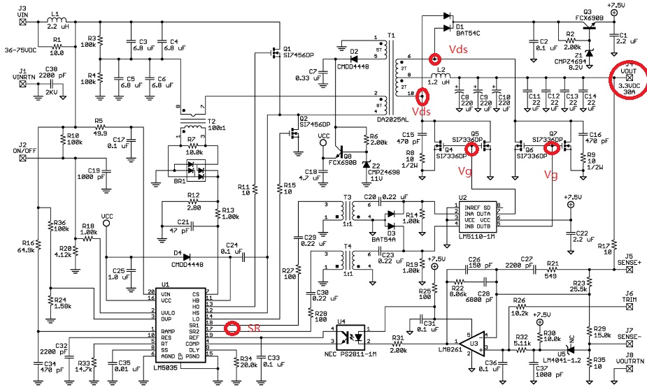
As shown in the figure below, I tested the waveform of the prototype at full load.
Yellow is the input voltage Vin waveform, green is the output voltage Vo waveform, purple is the output current Io waveform, and blue is the DS terminal waveform of the secondary rectifier MOS tube.
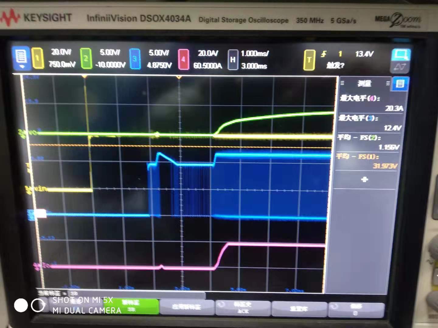
Before the output voltage gradually rises from 0V to 5V, Vo and Io will have a cluster of small pulses and Vds will be turned on. I do n’t know why this cluster of pulses is generated.
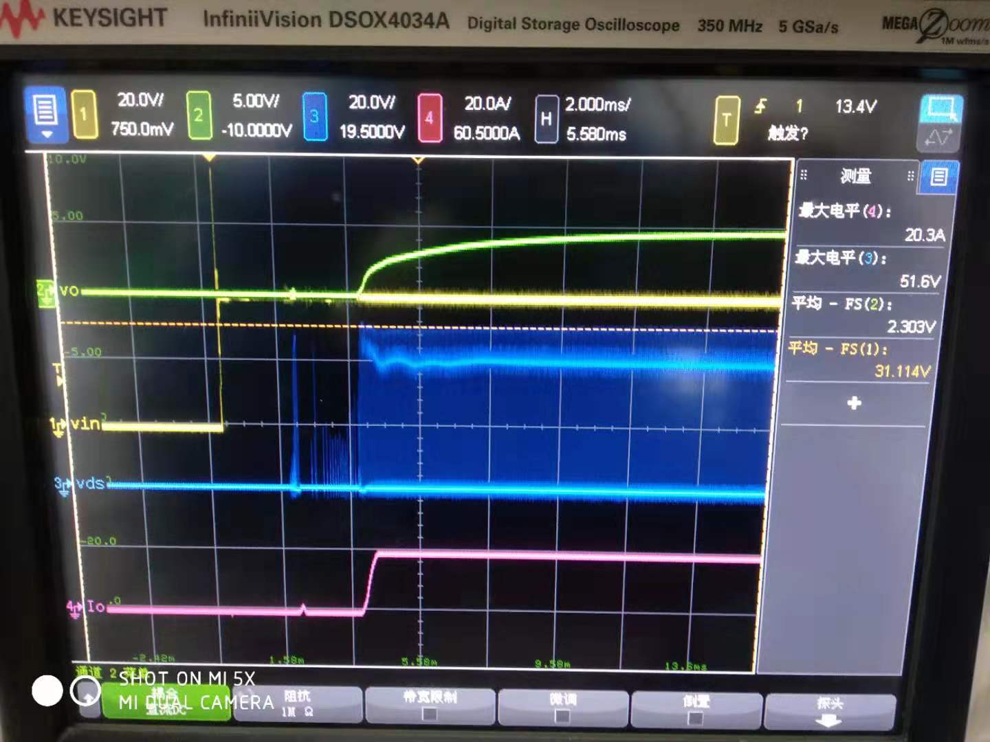
The blue picture below shows the Vg waveform driven by the secondary synchronous rectifier.
Before normal startup, there will be a cluster of trigger signals.
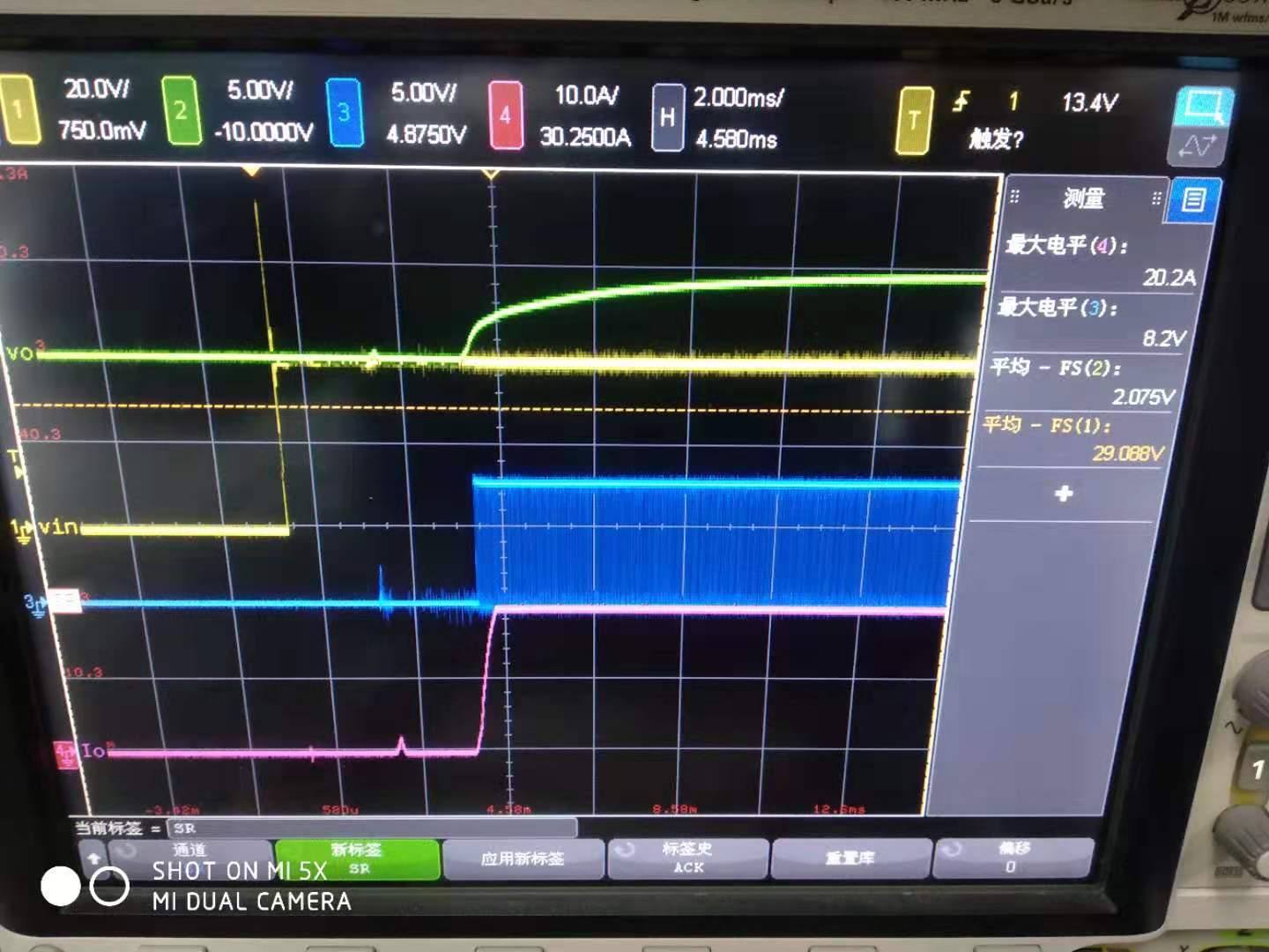
The blue picture below is the SR waveform of the LM5035.
How to eliminate this abnormal driving signal?
thanks.
