Is there a normalized thermal impedance chart for the Junction to Ambient scenario for this device.
This thread has been locked.
If you have a related question, please click the "Ask a related question" button in the top right corner. The newly created question will be automatically linked to this question.
Is there a normalized thermal impedance chart for the Junction to Ambient scenario for this device.
Hi Jack,
Thanks for your interest in TI FETs. TI provides max values for RthetaJA and RthetaJC in the datasheet along with normalized transient thermal impedance curves for pulsed power applications. During characterization, we test a small number of samples to obtain the values in the datasheet. The D2PAK is actually tested in open air like a TO220 thru-hole package. We have also done thermal modeling to determine RthetaJC to the top of the package. Typical value is 30C/W. You can find more information on thermal impedance at the blog listed below. Please let me know if you have additional questions or need more information.
Hi John,
As I understand it, the Normalized Impedance chart in the CSD19536KTT datasheet is for R_theta_J_C and cannot be used as an approximation for R_theta_J_A, is this correct?
Essentially I have two events I am worried about for this FET based upon a device I am using to control it. These events occur on the ~2.4ms timeframe and I cannot accurately justify the FET "safety" if I am trying to use the SOA curve. I was looking to use the Normalized Impedance chart for R_theta_J_A to determine if the rise in temperature at our pulse was acceptable given the requirements I have placed upon my designs or as a justification for if the FET will survive.
Am I going about this properly, or is there something I am missing here? Thanks for the help on this.
Hi Jack,
TI only provides transient thermal impedance plots for junction-to-case and those are not applicable for junction-to-ambient. That is because junction-to-ambient includes the part we can control (junction-to-case) and the part determined by your PCB design and stack-up (case-to-ambient). I did some checking and the only ZthetaJA data I could find is for a FET in a TO220 package in free air inside a temperature chamber. You can see how this is tested in Figure 2 of the blog I referred to in my previous response. Very different from a D2PAK surface mounted on a PCB. If you're interested, I can send this to you in a private message. I will send you a friend request.
Can you provide any additional information about your application and the two events that you're worried about? If you do not want to share it on this public forum, we can do it via private message or regular email.
Hi John,
My apologies, I can be a bit more specific with the numbers that I am looking to verify.
Essentially, the event that will be most stressful for the CSD19536KTT device in our application is around 370W @ 26VDC for ~2.4ms. I am just looking for a way to verify this will be okay for the device given the SOA curve does not have a 2.4ms trace.
Thanks,
Jack
Hi Jack,
Thanks for the clarification. Sorry if I rambled on a bit in my last response. Unfortunately, our SOA tester only does powers of ten for pulse widths and 2.4ms is in between the 1ms and 10ms curves. I pulled up the SOA test data and at 26V, the SOA current is 44.5A (1156W) at 1ms and 13.8A (360W) at 10ms. It's pretty close to meeting your requirements at 10ms. A few things to note:
You're a lot closer to the 1ms line than the 10ms line. I think you're going to be OK but you probably want to run thru the calculations yourself. Here's another blog on SOA testing and specification for TI FETs.
John,
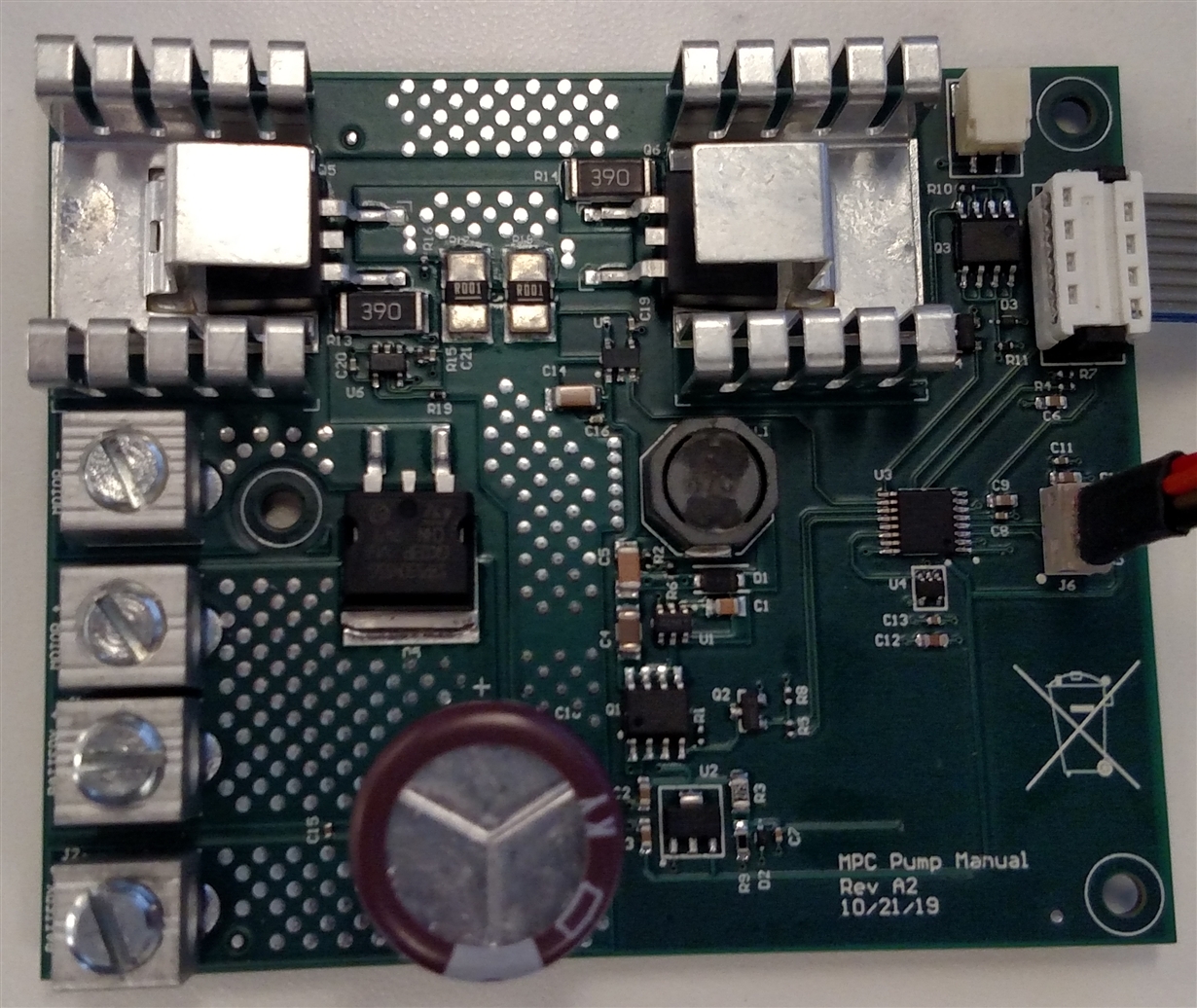
I to am using the CSD19536KTT MOSFET, and have questions about the thermal impedance. I have two of the MOSFETs on a board, top layer and bottom layers are 4 oz copper areas of 575mm2 for a total of 1150mm2 area with 4 oz copper (for each FET). I also have 2 inner layers of 1 oz copper of the same area to give me a total 1 oz area of 1150mm2 (for each FET). Also have heatsinks on top side on both MOSFETs (see attached photo). Trying to determine how much continuous current I can pump through the FETs before the junction temperature is an issue. In your previous response to John Wallace you gave a number of 30C/W for junction to case to the top of the package, would this be a good number to use. I can measure the top case temperature and trying to determine what junction to case (top of case) number to use to determine junction temperature. Any other suggestions on how I can determine this would be appreciated.
Regards,
Larry A. Gunseor
Hi Larry,
Thanks for your interest in TI FETs. TI has modeled some of our FET packages including the CSD19536KTT in D2PAK. From these simulations, we have determined that RthetaJC(top) is ~30degC/W. I suppose if you measure the temperature on top of the case, you could back calculate to determine the junction temperature. However, not all of the heat is going to be dissipated thru the top of the case. In fact, looking at your board, it appears that the predominant thermal path is thru the tab of the device into the PCB and to ambient thru the heatsink mounted on top of the board. You can probably model this using Flo-Therm or Icepak. Of course, you can test it as well. In order to calculate the maximum current you can put thru the FETs, we would have to determine the effective RthetaJA. Again, this can be done empirically. Below are links to some useful blogs and a thermal application note. The first one is on thermal impedance and the second is on maximum continuous current. The app note is pretty self-explanatory. Please contact me if you have additional questions or need more information.
Hi John,
All this information has helped greatly, I believe I can justify the derated values based on the numbers you have presented.
Would you also be able to tell me the numbers for 28V at 1ms & 10ms?
Thank you for the help.
Jack
Jack,
John is away on vacation for the next week or so so I will jump in to try and help.
I am not entirely sure what you are asking, do you want to understand the SOA capability of the FET, this can be read from the datasheet fig 10, or are you looking to adjust the thermal impedance of the MOSFET using fig1 of the datasheet?
Jack,
Unfortunately these specific data points you are requesting are no in the report, as such I would recommend using the log curve int he datasheet and eye balling it.
I did this myself and would estimate 28V 1ms to be 35A, 10ms to be just over 10A, say 10.2A