This thread has been locked.

If you have a related question, please click the "Ask a related question" button in the top right corner. The newly created question will be automatically linked to this question.

LM5122: Operating in continuous mode with a wide Vin/Vout ratio

Part Number: LM5122

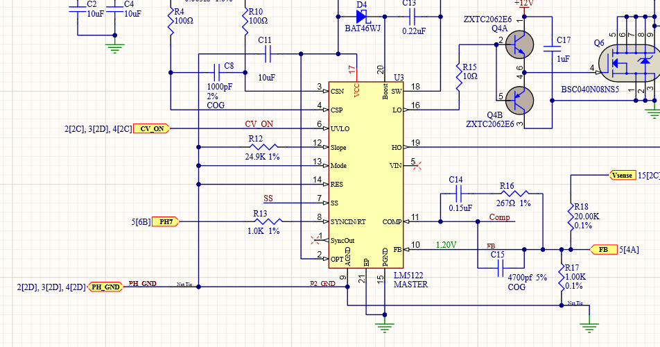
I have two designs with this IC (LM5122), a 20V to 27V, 8 phase, 3.2KW converter and a 26V to 54V, 8 phase, 3.2KW converter. Both are operational and stable. The first configuration has had several 1000 units in production with no issue.

I am attempting to develop a 20V to 45V, 8 phase, 3.2KW converter based on the first design.

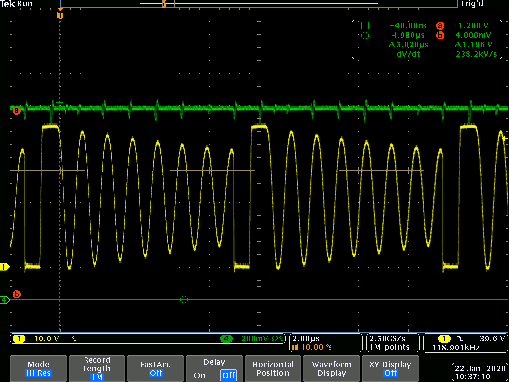
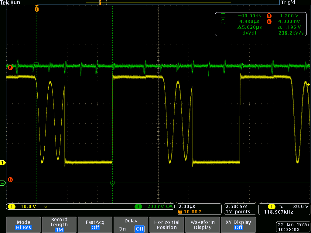
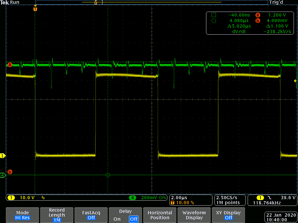
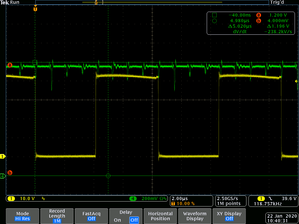
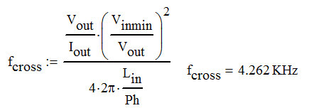
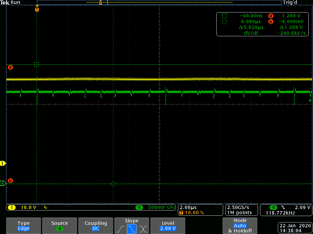
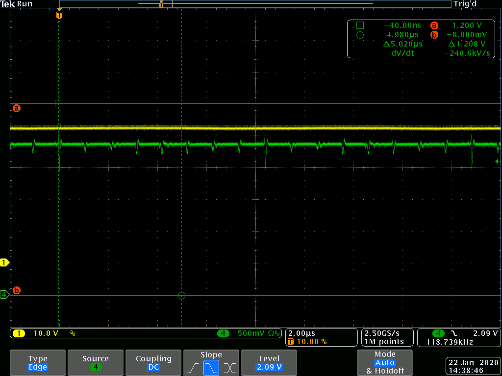
My first several attempts had issues with voltage regulation in continuous mode. In discontinuous mode the regulation is good, but falls about 5% when all 8 phases go into continuous mode, and continues to sag with more load. The converter is NOT power limited and it is stable. The voltage across the bottom regulation string resistor is 1.2V and starts to sag when it goes continuous.

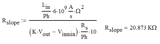
As a work around I have resized the main inductors to stay in discontinuous mode under all load conditions. I have changed the current limit filter and compensation all over the place with little to no effect. The only filter configuration that worked was when my tech misunderstood instructions and changed the current input resistors to 30K (from 100 ohms) with a 2200pF cap. This configuration had acceptable regulation (2%) over the full load profile but I'm reluctant to operate with this filter configuration for obvious reasons.

What am I missing to get this configuration to work in continuous mode?

  • Hi William,

    Thanks for reaching out with your question and for using the LM5122. Sorry to hear you are having issues.

    Is it possible to post the schematic? This will help me resolve the issue.

    Thanks,

    Garrett

  • I will attach 3, 780-116533F 27V Converter.pdf

    780-115696B 54V Converter.pdf

    143309A 36V Reworked Converter.pdf

    The first two work, the last is the one I'm having issues with.

  • Hi William,

    It sounds like this might just be related to the control loop compensation.

    First please set the current sense filter back to normal, IE a non 30kOhm value. Then please try the following (I am refering to 143309A_36V_Reworked_Converter.pdf

    1. Change R17 to 900 Ohm
      1. This will set the output to 45V
    2. Loop compensation
      1. Change the following values to improve the phase and gain margin

                                                                   i.      R16 = 680 Ohm

                                                                 ii.      C14 = 100nF

                                                                iii.      C15 = 3.3nF

    1. Output Capacitors
      1. Make sure that these are 100V rated.
    2. Ceramic capacitors loss effective capacitance when a DC voltage is applied. This can reduce the capacitance as much as 80% for some ceramic
    Please let me know if you have any questions.
    Thanks,
    Garrett
  • Garrett,

    Your values got us closer, but still not there yet.

    Vout
    R16=680, C14=100nF, C15=3.3nF Output Caps= 63V

    Rslope 30.1K
    I filter
    2X 100Ω
    1000 pF
    Isense=2.22mΩ    20uF Input Cap & 50uF Output Cap

    37

    42.91

    42.93

    42.71

    42.17

    41.7

    41.26

    f=119kHz

    Vin=22

    Vout=43

    We did not change R17 since we inject a DC voltage into the feedback node to control the output voltage. See page 5 of the schematic.

    Next steps?

  • Please ignore the "37" in the first row, this is the iteration or modification number.

  • I should have sent the entire table.

    I out

    Rev. B PCB            Vout
    Rslope 30.1K
    I filter
    2X 100Ω
    1000 pF
    Isense=2.22mΩ    20uF Input Cap & 50uF Output Cap

    Vout
    R16=680, C14=100nF, C15=3.3nF Output Caps= 63V

    Rslope 30.1K
    I filter
    2X 100Ω
    1000 pF
    Isense=2.22mΩ    20uF Input Cap & 50uF Output Cap

    Iteration

    31

    37

    0

    42.85

    42.91

    10

    42.84

    42.93

    20

    42.46

    42.71

    30

    40.87

    42.17

    40

    40.46

    41.7

    50


    41.26

    f=119KHz

    f=119kHz

    Vin=22

    Vin=22

    Vout=43

    Vout=43

  • While I'm waiting for your response, here is another question I have.

    What effect does the number of phases have on the slope compensation and loop compensation equations?

    Through experimentation I have discovered that the maximum switching frequency is 1MHz/#phases. This means that the maximum switching frequency/phase for an 8 phase converter is 120KHz (120KHz*8 phases = 1MHz).

  • Hi William,

    When you say the output capacitor is 50uF, is this the total output capacitance of all 8 phases? Or is this the single phase output capacitance?

    Also can you probe the FB pin voltage and the COMP pin voltage? This will let me know if the converter is regulating. Please post a screen capture of the output voltage. I want to see if the output voltage is oscillating at all.

    The impact to the number of phases on the loop compensation is explained in table 2 foot note 2 of the datasheet.

    Thanks,

    Garrett

  • Garrett,

    40 X 10uF, 63V (now) MLCC, 5/phase, see schematic.

    Waveforms requested;

    File

    Output Current (Amps)

    Ref. Designator

    tek0008

    0

    R17

    tek0009

    10

    R17

    tek0010

    20

    R17

    tek0011

    30

    R17

    tek0012

    40

    R17

    tek0013

    50

    R17

    Note green cursors @ 0V and 1.20V (chip reference). Yellow trace is across boost fet phase 1.

  • I discovered the note of table 2. I notice the phase number, or "n", cancels out if you plug the equation:

    into;

    They also cancel out in the Rslope equation;

    What about the Rslope minimum equation? Neither the inductor nor the sense resistor appear.

  • Waveforms continued;

    File

    Output Current (Amps)

    Green Waveform

    Yellow Waveform

    tek0006

    0

    Comp pin

    Output Voltage

    tek0001

    10

    Comp pin

    Output Voltage

    tek0002

    20

    Comp pin

    Output Voltage

    tek0003

    30

    Comp pin

    Output Voltage

    tek0004

    40

    Comp pin

    Output Voltage

    tek0005

    50

    Comp pin

    Output Voltage

    I have noticed the comp pin is not linear to the current. Seems to be a logarithmic response.

  • Hi William,

    The slope resistor doesn't need to change with the number of phases. The slope compensation is needed on each phase . Note the slope compensation is related to the falling slope of the inductor current and the sensed current for each phase.

    How are you probing the COMP pin? I looks like there is a lot of switching noise getting injected onto the pin.

    Thanks,

    Garrett

  • We used an active probe, Tek P6243, between the node of C14/C15 and phase ground.

  • Hi William,

    Can you please try adding a capacitor to the VIN pin of every LM5122? I just realized that part is being powered through VCC and there is some internal circuitry that is powered from the VIN pin. Please try with 0.1uF.

    Thanks,

    Garrett

  • Garrett,

    There was no difference when we added the cap.

    We have been able to improve the operation by changing the compensation with the assumption that the output caps dropped to 2uF with the 43V DC bias (from 10uF). The compensation components become;

    Ccomp = 0.047uF

    Rcomp = 243Ω

    Chf = 680pF

    There is still a large drop in the output regulation as the IC warms. In the table below the first column is without the cap, the second column is with the cap at startup. The third column is after 5 minutes of running @ 2KW.

    I out (Amps) Vout                 Rslope=20k
    R16=243, C14=47nF, C15=680pF   Output Caps= 75V
    Vout                 Rslope=20k
    R16=243, C14=47nF, C15=680pF   Output Caps= 75V 0.1uF From Pin 5 (Vin) to AGND all phases
    Vout                 Rslope=20k
    R16=243, C14=47nF, C15=680pF   Output Caps= 75V 0.1uF From Pin 5 (Vin) to AGND all phases.                 After 5 minutes running at ~2000W
    Iteration 56 57 58
    0 42.93 42.93 42.91
    10 42.92 42.91 42.92
    20 42.88 42.87 42.83
    30 42.12 42.42 41.96
    40 41.97 42.29 41.87
    50 41.48 42.07 41.56
    Frequency f=119kHz f=119kHz f=119kHz
    Input Voltage Vin=22 Vin=22 Vin=22
    Output Voltage Vout=43 Vout=43 Vout=43
    ΔV from setpoint 0.96 0.64 1.04
    ΔV % 2.2% 1.5% 2.4%

    As you can see there is a large drop-off in regulation as the IC warms up. This is also shown in the previous waveforms as a drop in the voltage across R17 (Vref).

  • H Will,

    I sent you a personal message so we can discuss this further. Please contact me the message boards.

    Thanks,

    Garrett

  • Garrett,

    Please try again, I can't seem to find the message.

  • William,

    Did you see the friend request that I sent you? Accept this and then we can message directly.

    Thanks,

    Garrett