This thread has been locked.

If you have a related question, please click the "Ask a related question" button in the top right corner. The newly created question will be automatically linked to this question.

TPS7B7701-Q1: Reverse Current detection in Switch Mode

Part Number: TPS7B7701-Q1
Other Parts Discussed in Thread: TPS7B7702

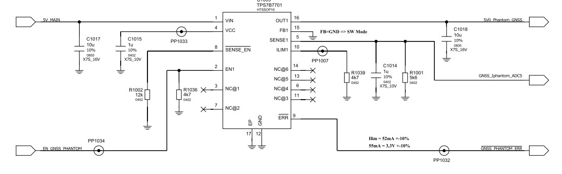
We use theTPS also in switch Mode and my Problem seems to be the same as described in  the Thread:


https://e2e.ti.com/support/power-management/f/196/t/807598?tisearch=e2e-sitesearch&keymatch=TPS7B7701-Q1%2520reverse%2520current

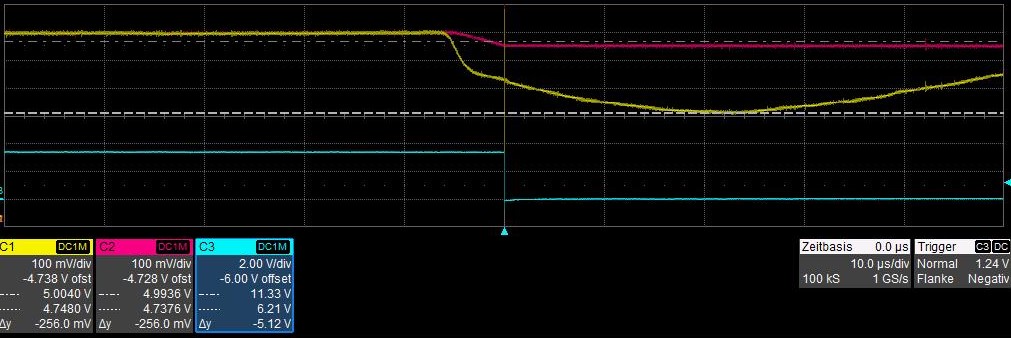
In the scope trace you can see how the output voltage (red trace) follows the input voltage (yellow trace) until the error output is set (blue trace).

Our Implementation is as follows:

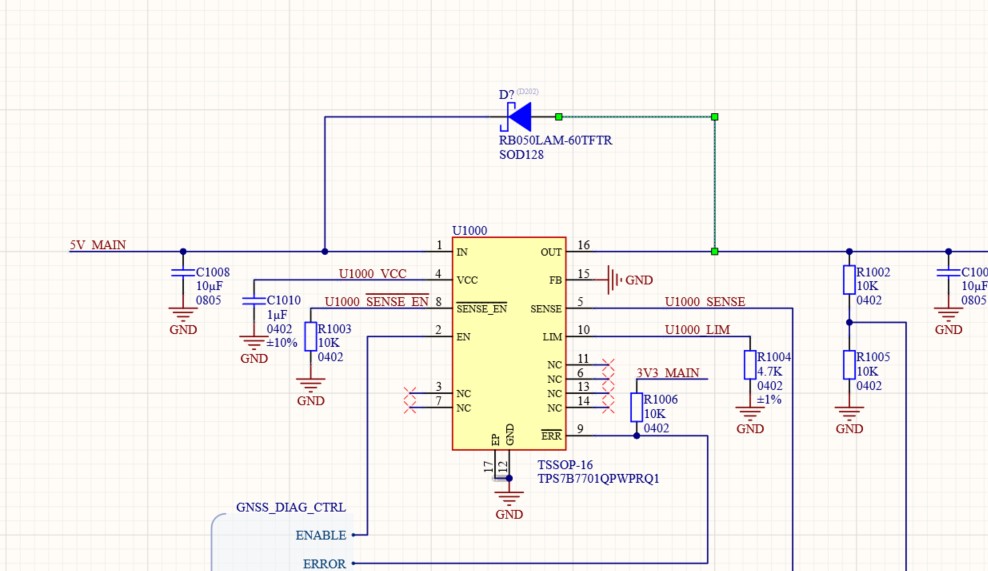
We also found that removing C1018 solves the issue and the output voltage immediately follows the input. In the thread mentioned above, its not finally clear if the capacitor is required. Is it possible to use a much smaller value (e.g. 100nF) if using the device in Switch mode to maintain full functionality of the IC? Or are 2,2µF the lower limit for the output capacitor?

Do you have any suggestion how to solve the issue without Diodes?

Best regards, Michael Möller

  • Hi Michael, 

    As discussed in the other post:

    The swiched-mode bypassing the control loop of the LDO and no output capacitor is needed for stability. However, the current limit loop may require a capacitor to operate. 

    We had a discussion here, and we would recommend having a 2.2uF capacitor or higher on the output even the device is used in switched-mode.

    Regards, 

    Jason Song

  • I tested with replacing C1018 with 2,2uF at the output. This improves the behaviour and the chip seems not to enter reverse current protection State, but the effect that the input voltage drops below the output voltage is still present. Below are three captures with 0, 2,2 and 10uF at the output.

    How can I be sure that with 2,2uF the chip will not enter reverse current protection under all conditions? Maybe I'm close to the limit and getting a bord with higher tolerance witll enter the error state, even with 2.2uF. Can you please provide how to validate that the reduction to 2,2 uF at the output is a sufficient measure?

    I always tried to increase the input capacity, but I found that the effect is only minmal when doubling to 20uF. to get a significant effect, I think I need to increase to a much larger capacitance which is not practicable in our desing.


    best regards,

    Michael Möller

  • Hi Michael,

    Your message has been received and thanks for providing updated scope-shoot, please allow some time for me to investigate on this issue, I will get back to you by 3/17. 

    Regards, 
    Jason Song

  • Hi Michael, 

    Thanks for providing the scope-shots with different output capacitors. I understand you are concerning about how much design margin you have with the 2.2uF capacitor without causing an unintended reverse current latch. 

    Other than increasing the size of the input cap, is there another way for you to slow down your input supply when powering down? What is driving the input of the TPS7B7702?

    Regards, 
    Jason

  • tHello Jason,

    thank you for the reply. The input of the TPS is driven by a 5V DC switching regulator.

    The voltage drop is not caused as result of a switch off event.

    There are several other sinks on this supply and one has high load current transients (>= 1A). These transients cause the voltage drop. The drop was measured at the TPS input and is the combination of the regulator load transient response and the lossed caused by the PCB trace impedances....

    Unfortunately the drop is caused multiple times each second when the system is running and after a certain while (about 1-2min.) the TPS goes into the error state.

    Best regards,


    Michael

  • Hi Micheal, 

    Thanks for sharing the information about  your application. Do you think you could try to have a schottky diode between the output pin and the input pin and run some tests? The diode need to have a lower turn-on voltage and this will help discharging the output and charging it back to the input to reduce the chance for a RC detection by the internal circuitry. 

    Regards, 
    Jason Song

  • Hello Jason, 

    you mean that the ouput capacitor can be discharged via the diode? In this case, the reverse current blocking of the IC would not work because the reverse current will 

    conduct over the diode path, or am I wrong in my understanding? 

    I understood you request like this:

    best regards,

    Michael Möller

  • Hi Michael,

    Yes, if you have the diode as shown in the schematic, the external diode will discharge the output to Vin to prevent the device from triggering its internal RC protection that will latch the output. As we discussed, there is little thing you could do to slow down your input droop and a 2.2uF is required for the stability of the LDO.

    Will this meet your needs?

    Regards, 
    Jason Song

  • Dear Mr Song,

    Thank you for your reply. My current understanding is that even with the recommended 2,2uF on the output TI cannot guarantee the functionality if using the IC in Switch mode.

    All workarounds suggested were workarounds which allow operation only with limitations in functionality e.g. no reverse current protection or additional forward voltage drop.

    In my opinion this means that the IC cannot be used as switch as it is described in the datasheet. Therefore I need to find another solution for further designs if you cannot suggest a

    solution guaranteeing the full functionality without restricting device functionality.

    best regards,


    Michael Möller

  • Hi Michael, 

    Instead of having the external diode, will it be possible to add a resistor from the output to the ground that will pull down the output faster during the power down? It will be much easier to implement and it will help to create an additional margin with the 2.2uF output capacitor. 

    We understand you don't like workarounds to make the device work for your application. But each application is different and most of the switching application does not have fast Vin ramping as the one existing in your application. Having an external diode or an additional pull-down resistor at the output will help to create the additional margin with the 2.2uF output in switched-mode. 

    I have provided your feedback to our design team and we will be doing the evaluation to hopefully lower the output capacitor requirement in switched-mode. I have last tested the device with the EVM, and at nominal condition, the device has no issue without the output capacitor. But before we can recommend this to our customers, we would need to complete our evaluation at different temperatures and corners. We are looking at the end of May 2020 timeframe to finish this investigation. 

    Regards, 
    Jason Song