This thread has been locked.

If you have a related question, please click the "Ask a related question" button in the top right corner. The newly created question will be automatically linked to this question.

TPS62745: TPS62745

Part Number: TPS62745

Hello,

We are facing similar situation.

Vsel was connected to Vin (design error), powered by batteries higher than 6V and some devices are damaged. 

Would be possible to share the squematic internally and go deeper on the severity of this problem?

Thanks in advance.

BRs, 

  • Igor,

    It is probably difficult at this time.  We can only recommend that teh abs max rating be observed.  I will contact our design team about internal details.  For sure it will require an NDA to share any details.

  • Igor,

    These pins connect two to pieces of internal circuitry: 5V ESD clamp, and inputs of 5V CMOS logic gates running on an internal rail.  The obvious mechanisms of damage that I can foresee from over-voltage on these pins include:
    ·         Damage to pin metallization or ESD clamp due to triggering of ESD cell.  This could cause functional issues with the VSEL signaling, as well as other possible issues if reflowed metal shorts to nearby circuitry.  This type of failure would be immediate when the overstress occurs.  In my estimation the risk of this kind of failure is low if the pin voltage stays below 7V, since the nominal trigger point for the ESD clamp is above 11V.
    ·         Damage to the gate oxide of the ESD cell or the CMOS logic gates.  This could cause functional issues with the VSEL signaling, as well as other possible issues if the high current flowing through the failed oxide loaded down the internal rail or caused reflowed metal shorts to nearby circuitry.  This type of failure has increasing probability of occurring as the time of exposure to over-stress increases.  The risk for this failure is also low if the pin voltage stays below 7V.  Our model for this kind of failure mechanism predicts less than 1 failed unit per billion after 100k operating hours at the worst case temp of 150C as long as the voltage never exceeds 7V (including transients, ringing, etc).  
     
    Of course, this assessment should not be taken as any kind of guarantee of results for the customer.  I have considered the most apparent mechanisms of failure under this application’s conditions, but this kind of analysis isn’t foolproof.  It’s possible that there could be another mechanism or issue that I have not caught, which is why we qualify and specify the components and circuits within a given range.  That more rigorous process yielded the abs max specs that are being violated. 
  • Thanks for your complete and so deep reply John.

    It seems that our board don´t have to face many problems working below 7V (maximum 1 per billion).

    After your answer, we have tested today 200 boards, just connecting 6,3 V Lithium battery, and 28 units are damaged, so current consumption increases 10-100 times. After changing TPS62745 regulator it works fine returning to the normal current consumption.

    So, do you think there is another possible problem, maybe on our schematic? Or could be possible to be a batch problem on these regulator, I don´t think so, but do you have any information about it? 

    Thanks in advance.

  • Igor,

    There are no lot quality issues that I am aware of.

  • Hello John,

    Thanks for your answer.

    So, if we are working under any probed specifications, there is no explanation for having to replace your regulators on some of our devices in order to work properly.

    If you are able we can share our schematic with you, maybe there is something wrong that we cannot detect.

    BRs,

  • Igor,

    if you post your schematic, I will review it.

  • Hello John,

    Attached you can find schematic referred to TPS62745. Where D1, D2 and T4 are not mounted. So J2-battery power go directly to R2 0 ohm. 6V lithium battery is connected to J2 in normal activity (initially 6,5 V).

    In parallel 3V3 are applied to Vout from TC1 connector when device is programming. Sometimes could be 3,4 - 3,5 V.

    Can you see any issue on that schematic?

    Thanks in advance.

    BRs,

  • Igor,

    If you apply an external 3.3 V to the output of the TPS62745, and the battery is not connected the high side body diode can conduct and you may possibly have enough voltage at the input to allow the device to start switching.  Can you check it in that condition?

  • Hello John,

    I have checked what you said and there are 0,25 V on the high side body diode along the range of 2-4V applied externally on Vout / SW pins.

    So, in normal situation, when we apply external 3,3 V at the V output we have 3,05 V at Vin pin.

    If we apply external 3,4 --> 3,15 V at Vin

    If we apply external 3,5 --> 3,25 V at Vin

    So, it could be a problem to damage the chip?

    Thanks

    BRs,

    Igor

  • Igor,

    Do you see any switching activity on the SW pin?  Is EN tied low?

  • Hello John,

    Attached you can find both signals when connecting 3,5 V to Vout, on an already damaged chip.

    Vout & SW --> GREEN

    Vin & EN --> YELLOW

    BRs, 

  • Igor,,

    If the part is already damage, then you will not see any switching.  I recommend you not apply any voltage above 2.5 V to the output unless you have the TPS62745 EN pin pulled low to ensure the device is disabled.

  • John,

    Here you have Vin/Vout signals when connecting 2V5 to Vout on a non damaged chip.

    Vin is 0,25V less than Vout, also decresing Vout to 2V.

    With Vin&EN pulled low, connected to GND, there is just 0,25V on this pin after connecting 2,5V on Vout. 

    BRs,

    Igor.

  • Igor,

    Yes as long as you have EN low, you are safe.

  • John,

    In our typical procedure, while programming the board by external 3V3 on Vout, EN is not low and couldn´t be low because Vout would be connected to GND through the high side body diode.

    It seems that applying some voltage to Vout-SW could damage the chip, if EN is high,.

    Am I right or is there any other conclusion?

    Thanks.

    Igor

  • Igor,

    Yes there is potential for damage if the applied output voltage is more than one diode drop above the input under voltage lock out and the device is also enabled.

  • Hello John,

    Undervoltage lockout threshold is 3,1 V. 

    Diode drop is 0,25 V

    We can apply 3,1 + 0,25 = 3,35 V minimum at the output for not damaging the chip. Is it correct?

    In this case, we would have 3,1 V at Vin & EN. It could be still a problem or there is no risk on this case?

    BRs,

    Igor.

  • Igor,

    That UVLO threshold is "typical".  It may be lower.  I would use 2.9 as the minimum threshold.

  • Hello John,

    We have tried to program the chip at 2,8 V and it works. So, we are going to program a bigger batch of boards, check the battery consumption and then I will let you know the results. I hope it should resolve this issue.

    In parallel i wanted to tell you that we followed the instructions of TI reference design and smart lock, using same regulator, as you can see in the following links:

    http://www.ti.com/lit/df/tidrmq3a/tidrmq3a.pdf

    http://www.ti.com/lit/ug/tidubv3c/tidubv3c.pdf

    It uses the same regulator and asks to connect the board with CC2640R2 directly from the programmer at 3V3. Same than we did.

    Having in account UVLO threshold, it seems that there is a mistake on this TI design reference. Please confirm that in order to avoid future similar issues on new designs.

    Thanks.

    BRs,

    Igor 

  • Igor,

    So long as the output is pulled high enough that VFB is higher  than the reference, there should not be any risk.  I cannot comment about those other designs.  Our group did not design them.

  • Hello John,

    Thanks.

    What do you mean with VFB?

    We are below 2,9 in Vout to avoid problems, as you asked.

    BRs,

    Igor

  • If VFB is higher the the Internal reference voltage, the IC will not switch and there is no possibility of it boosting up the input.

  • Hello John,

    Thanks. VFB is V_TH_UVLO?

    V_TH_UVLO minimum value is 2,9 V. This is why we have powered 2,8 V at Vout for chip programming, so Vin should be maximum 2,55 V. 

    After programming a batch of 200 units at 2,8 V we have less regulators damaged: 6%, but the problem is still there.

    Is there any other reason to explain that problem?

    BRs,

    Igor.  

  • I should have called it VOUT rather than VFB as TPS62745 has fixed programmable outputs.  If you are still having failures, I suggest you monitor the SW and VIN pins during programming to look for abnormal voltages or switching activity.

  • Thanks for the explanation John.

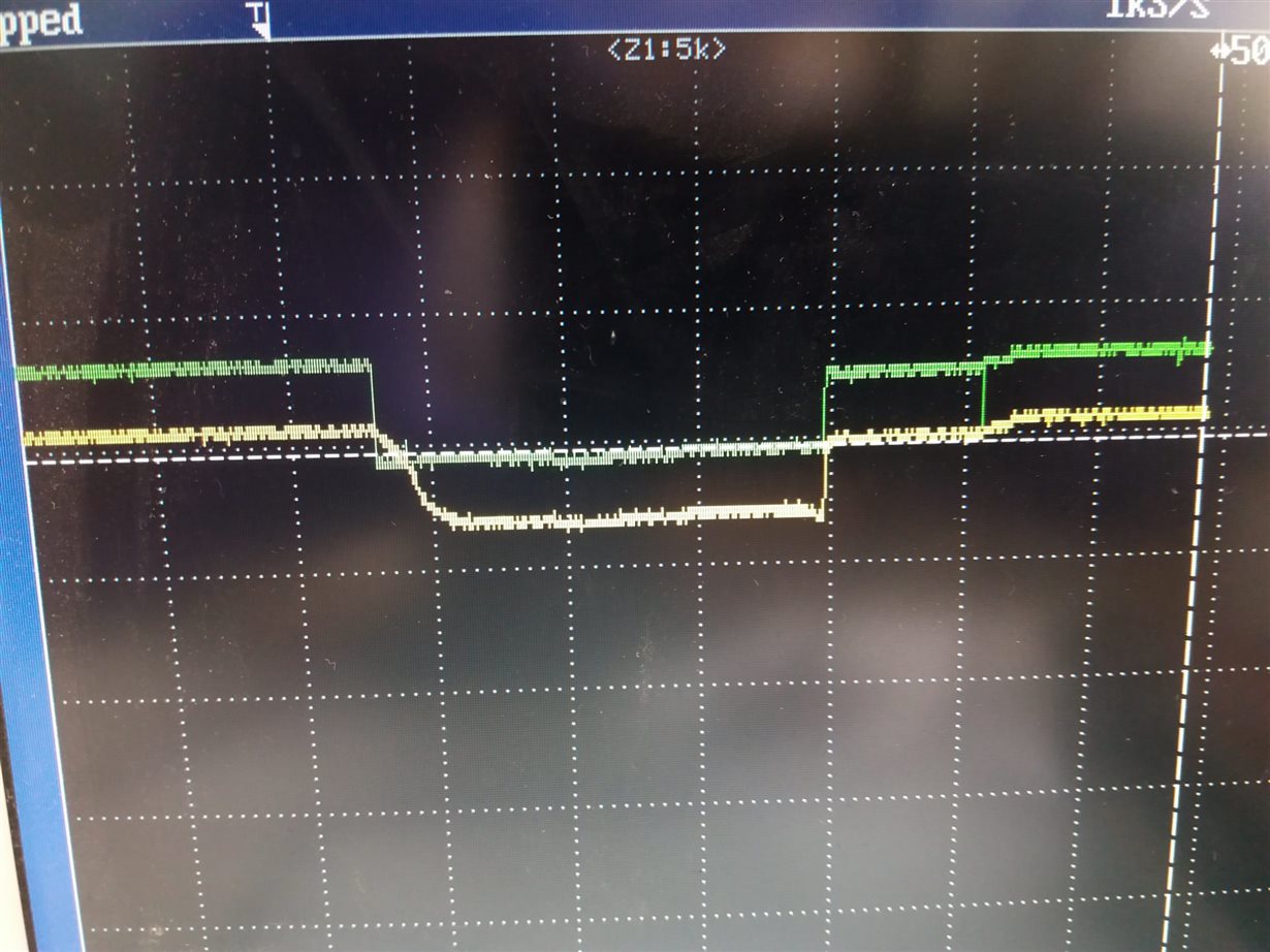
    Both signals are stable during programming:

    SW=2,8 V

    Vin=2,55 V

    After that, we make a system test, where SW voltage decreases below Vin during 100 msecs aprox. as you can see in the following picture:

    Is it a problem?

    BRs,

    Igor

  • Igor,

    I would have expected just DC voltages.  It is difficult to comment without being able to see the amplitude and time scales as well as the ground reference point.

  • John,

    Green signal is Vout=SW. 2,8V

    Yellow signal is Vin. 2,55V

    During the test, Vout decreases to 2,4 V, and stays below Vin, during 100 msecs, until Vin decreases also 0,4 V (0,25V below Vout).

    Scales are 500 mV / 500 msecs.

    BRs,

    Igor

  • Igor,

    Why do the voltages change?

  • Hi John.

    Voltages change because some LEDs are blinking during system test.

    I have been doing same procedure: to power the reader through regulator-Vout to 2,8V and do system test, but after testing 200 readers, Vout doesn´t decrease below Vin on most of the cases.

    So, regulator Vout & Vin are stable during programming and also system testing.

    There is another reason for damaging the chip...

    Are you doing any internal test to reproduce this failure?

    BRs,


    Igor

  • Igor,

    I am transitioning out od the support role for these devices.  Our applications manager will assign someone to pick this up.  I don't think this can be easily replicated here.  It seems it may be unique to your programming sequence.

  • Igor,

    At this point, I think your best chance is to closely monitor your next batch of boards during programming to look for over voltage on VIN.