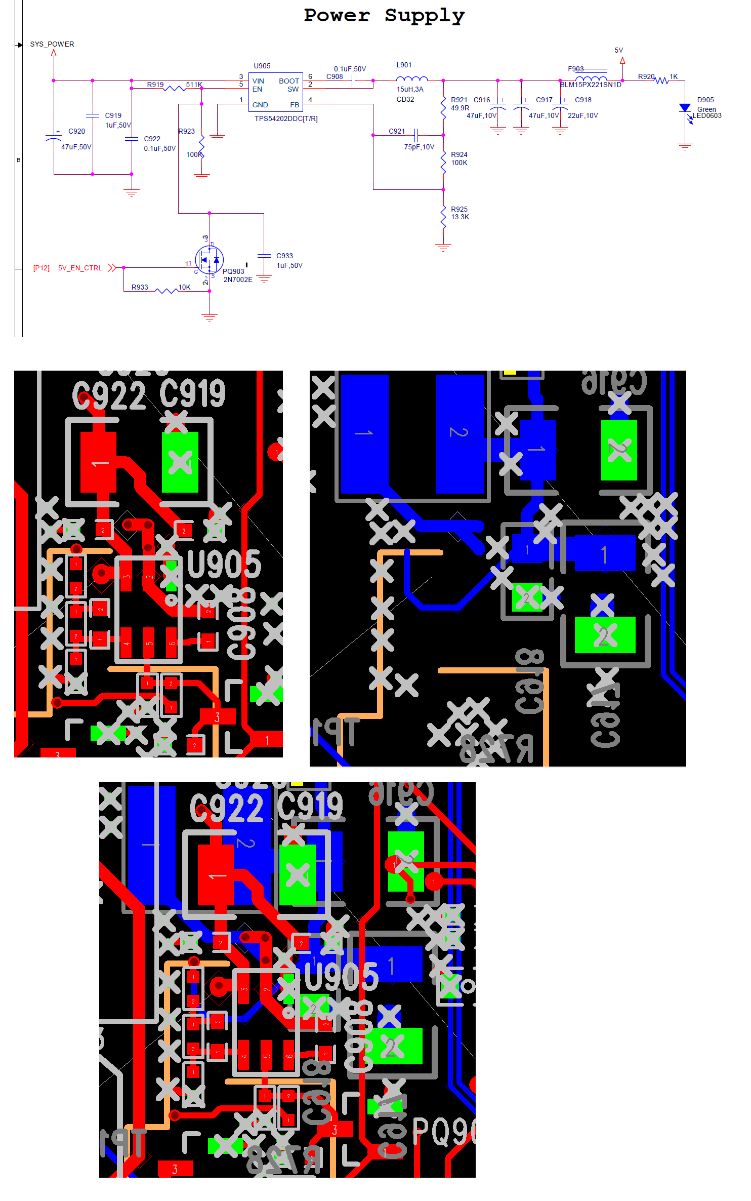
This thread has been locked.

If you have a related question, please click the "Ask a related question" button in the top right corner. The newly created question will be automatically linked to this question.

TPS54202: the VOUT and GND of TPS54202 is shorted immediately when 24V plug in sometimes

Part Number: TPS54202

Hi TI

I use TPS54202 to buck from 24V to 5V with about 1A.

And now we see some failures that the VOUT and GND of TPS54202 is shorted immediately when 24V plug in sometimes.

  this failue is not happened at the first Previous times, means those failure boards are worked before.

  this failure is not happened when 24V is already power on. means those failure boards worked normally if 24V can power oon successfully at that time.

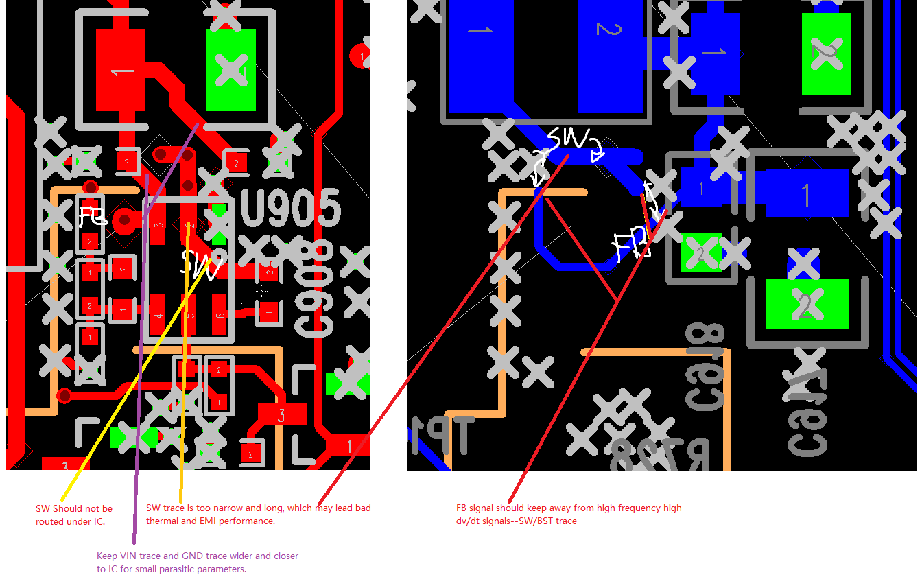
So, Could you please help me to check the schematic and layout below?

5V_EN_CTRL is always enable in this discussion.

the red is top layer and blue is bottom.

Thanks

  • Former Member
    0 Former Member

    Hi Cun,

    Could you please capture the input voltage waveforms near the IC to check if any overspike during the hot-plug in process?

    The over spike during the hot-plug-in process may damage IC.

    You can refer the appnote for more detailed analysis on the overspike during hot-plug in process: 

    Adding a TVS diode and an electrolytic capacitor with more ESR should be the solutions here.

    For the layout review, I would like to recommend you referring the example below:

    1. The input capacitor should be placed as close to the device as possible to minimize trace impedance
    2. The 0.1-µF ceramic bypass capacitor should be as close as possible to VIN and GND pins.
    3. Keep complete ground plane under the IC
    4. Keep the SW trace as physically short and wide as practical to minimize radiated emissions.

    Thanks.

  • Hi Bruce

    Thanks for you reply

    I will check the power when plug in and the capacitor also.

    for Ground, my board is a 6 layer board, and the layer 2 and 5 are both whole Ground plan, so I think the ground is strong enough.

    From you view, my IND which on bottom side is not a high risk, but the capacitor and something near the VIN should be high risk in my design, right?

  • Former Member
    0 Former Member in reply to Cun Lee

    Hi Cun,

    Please check my inputs below:

    1. SW trace should not route under the IC, or IC will be more easily coupled by this high frequency high dv/dt signal
    2. FB trace should keep away from high frequency high dv/dt signal--SW/BST trace.
    3. SW trace is too narrow and long, which will lead bad thermal and EMI performance.
    4. Keep VIN trace and GND trace wider and closer to IC for small parasitic parameters.

    I strongly recommend using the layout i attached before. Thanks.