This thread has been locked.

If you have a related question, please click the "Ask a related question" button in the top right corner. The newly created question will be automatically linked to this question.

TPS650864: SW2 does not work correctly

Part Number: TPS650864
Other Parts Discussed in Thread: CSD87381P, BOOSTXL-TPS650861, CSD87331Q3D, IPG-UI, USB2ANY

Dear expert,

Months ago, thanks to your help, we found the soldering issue for our TPS650864 evaluation board through this thread https://e2e.ti.com/support/power-management/f/196/t/875459. After re-soldering the board, we got the new board.

In the test, LDO5V5, and LDO3V3 are both correct. When probing the SW2 output, which is expected to give 0.85V, it seems not to work correctly. The output voltage is not stable, jumping from 0.5V to 4V, back and forth and the total current varies from 0.1A to 0.4A with the input voltage being 12V. And the chip is kind of hot. Due to the SW2 unnormal state, the other power rails have no output.

My questions are as follows:

1. What factors may lead to SW2 unnormal state? As a newbie to the TPS650864 chip, any advice is welcome.

2. If we would like to cut off the SW2 and let the other power rails work, how to achieve it? We had a try, in order to make SW1 work, pull high on CTL4 alone, but it does not work.

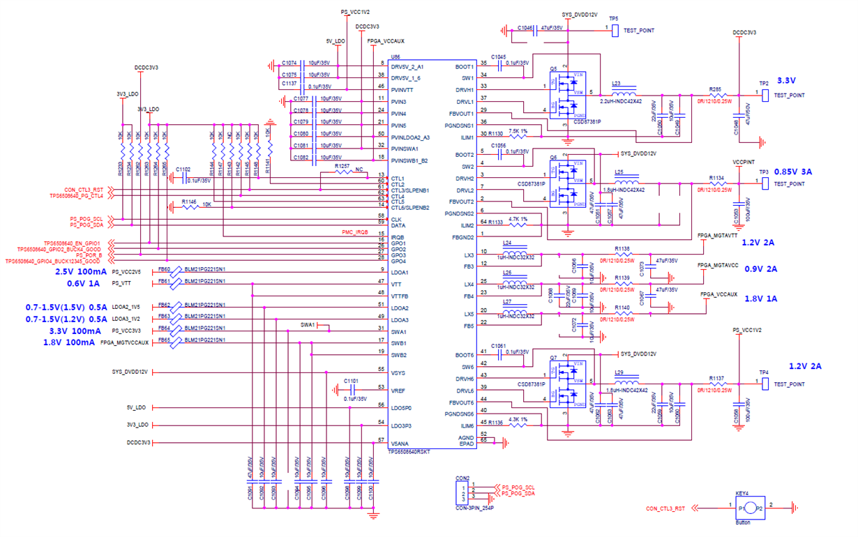
3. Could you help to check the circuits about SW2 as the following schematic?

Thanks ahead

  • Hello,

    The BUCK2 output could be unstable for a few reasons. I will try to list a few as well as a few ways to debug them.

    1. I always recommend posting the oscilloscope shots of the output. It it hard to provide any guidance without being able to see the specific behavior ocurring.
    2. Make sure it is BUCK2 that is the problem - we have seen many cases where we think it is one regulator when it turns out to be unrelated.
      1. Example 1 - I don't think it applies here, but the most common issue we see is that one of the other regulators does not have its proper external components populated and that is causing a power fault that shuts down all regulators. Any time any regulator in the chip has a power fault, the PMIC does emergency shutdown which disables every voltage regulator. So if LDOA1 for example was missing an output cap, that could explain shutting down. It would not lead to BUCK2 > 0.85 V though.
        1. Debug steps - take scope shots of the full sequence shown in Figure 6-4 and identify which rail is not powering up as expected. For your case, I would not start here but look at other items first.
      2. Example 2 - Another external regulator voltage is leaking onto the FBVOUT2 net. 
        1. Debug steps - Take a scope shot of the BUCK2 SW2 and FBVOUT2 during start-up. For TPS6508640, this would be after setting CTL3 high. Keep CTL4 low to ensure no other regulators are enabled. If there is voltage on FBVOUT2 before the buck is enabled, or if there is a sudden spike well after start-up, this would suggest an external voltage is backfeeding the PMIC. This is usually through some unexpected path in one of the ICs on the board.
    3. Soldering issue - we discussed this in previous thread but if any of the pins are shorted to any of the other pins, abnormal behavior will occur. The CSD87381P has best in class performance due to its unique package, but I've had several EVM builds come back with improper soldering of this FET. 
      1. Debug steps - when powered off, check the resistance between all of the pin combinations for shorts:
        1. DRVL, DRVH, BOOT, SW, FBVOUT, FBGND2 (so check DRVL - DRVH, DRVL - BOOT, DRVL - SW, etc) - it's a lot of tests but it's something the board manufacturer normally does.
    4. Current Limit at Low Negative Current - For cases where the voltage is rising above expected value, I typically look at current limit first. The peak current limit also serves as a negative current limit to protect the LS FET from being damaged. For cases where the overall current is fairly low, the negative current limit should be taken into account. It is detailed in Section 6.7.5 Current Limit of the datasheet, near the bottom. 
      1. Debug steps - remove the ILIM resistor and see if the issues is fixed. If so, increase the ILIM resistance or reduce the ripple current
      2. Note: PGNDSNS being connected to the power pad instead of the LS FET GND is a common layout mistake that results in less accurate current limit sensing.
    5. Too little capacitance - If there is not sufficient capacitance on the output, even a few pulses of the HS FET can cause significant overshoot. It depends on the inductance as well, but it has been an issue. I think the schematic shows 100 uF which seems fine. I don't like that it is after the 0 ohm resistor though, the FBVOUT may be very noisy.
      1. Debug steps - look at the SW node and FBVOUT2 waveform. If a single pulse causes the voltage on the output to jump, then there is probably too little capacitance.
    6. Layout - Hard to quantify, but if there is bad Vin or GND connection on the FET or SW to inductor connection, then the regulation could fail. Soldering issues could also be due to incorrect footprints / solder mask, etc.
      1. Debug steps - make sure the connections for each of these are very solid
    7. Insufficient supply - if any of the input supplies are failing, the regulation will not work
      1. Debug steps - check the input voltage to the FET as well as VSYS pin of PMIC and DRV_x_x pin on oscilloscope while observing SWx failing.

    Good luck and feel free to post updates for us to provide feedback.

  • Hi Kevin,

    First, many thanks for your detailed and expert advice.

    Following your advice,we do the debugs as follows.

    1.  Keep  CTL4  low to ensure the other regulators are disabled. LDOA1, LDOA2, LDOA3, SWA1, SWB1, and SWB2 are kept floated, without load. SWB1 and SWB2 are merged, which should be OK, right?

    2. When the 10V supply power is on, the total current reaches 0.3A, which seems to be large, and after a while, the chip becomes hot.  We can keep CTL3 low to disable the TPS650864. The output voltage is 0.412V.

    In the following picture, the top yellow is the output voltage(Vccpint) and the bottom green is SW, which is zoomed in the next picture.

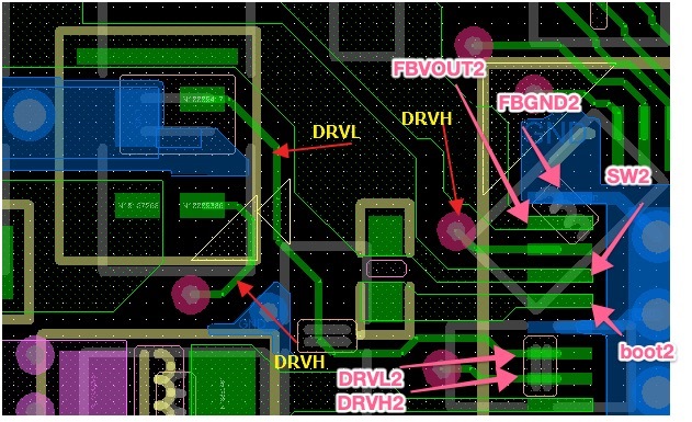
    3. This board is our evaluation board, so we choose 2-layer stack-up and do not pay much attention to the layout. There are some issues found in the layout. Can these bad layouts lead to SW2 not working correctly?

    1. FBOUT2 and FBGND are not routed as differential
    2. PGNDSNS is routed to the GND of TPS650864, not connected to LS FET GND directly, even though they are connected to GND finally.
    3. DRVH and DRVL are not routed on the same layer


    Thanks

  • Hi Chunjie,

    Let's stay focused on the case where CTL4 is forced to GND. In this case, only BUCK2 (VCCPINT in your diagram) is enabled. You mentioned 300 mA current draw from 10V supply - this is more than anticipated for a single buck regulator. I would expect roughly 30 mA. Is the 300 mA also true when CTL3 = GND? If so, there is either other current sinks than the PMIC, or we need to look at soldering again.

    The switching wave form looks a bit unstable and the 500 mV is clearly lower than target. The three layout issues you highlighted do not seem to me big enough to cause this issue.

    If possible, could you share the full layout in source format? I could then search for anything obvious. It can be messaged to me if that is preferable to posting (or you can post and we can delete it after I download). 

    I have never seen this device on a two layer board, so I have some concerns about power integrity, but I suppose it's plausible.

    If you are having trouble determining where the 300 mA is going, I would recommend a couple of experiments:

    Supply LDO5P0 with ~5.1V and see if the current draw goes away, that would indicate that there is excess current draw from that source, likely a solder issue, damage PMIC, or damage FET.

    Repeat with LDO3P3 with 3.4V.

    The scope shot is a bit low resolution to see anything happening on the switch node but the double pulsing is a bit unstable but not bad enough to cause Vout to be so low. 

    One layout issue I do see is the FBVOUT being routed so parallel with the SW node - this could be causing some noise injection, but again I would expect much lower.

    Is the DRV5V_2_A1 input cap right on the other side of the via on bottom layer?

    Did you try the ILIM resistor removal yet?

  • Hi Kevin,

    The current is definitely 300mA, which is large. When the CTL3 is GND, the current is 2mA, which is correct, I think.

    Do you mean to provide a 5.1V power from outside to the LDO5P0 so the outside 5.1v is parallel with LDO5P0? If misunderstanding, please correct me.

    DRV5V_2_A1 input cap is on the bottom layer and PMIC is on the top layer. For DRV5V_2_A1, there is a 0R resistor connected to LDO5P0.

    Removing the ILIM resistor is not done yet. What does this mean?

    I only have the gerbe file on hand. If it is not convenient,  please let me know and I will ask the original project file for you.

    In order to make it easy, we choose 2-layer board, however which seems not to be a reasonable choice:)

    power-gerber-20200218.rar

  • Hi Chunjie,

    You are correct regarding my intent for LDO5P0 / LDO3P3:

    Thank you for providing Gerbers. I think there may be some issues in my viewer, but I tried with two separate. In both cases, it showed the top solder for the PMIC pins as only having a tiny sliver of gap:

    It also had problems with the CSD87381P solder mask, it looked like the full GND plane was a single piece and very close to DRVL. If either of these are the case, the manufacturability of this board will be low. I'm still concerned we have a shorted DRVL given the extra current, but it could be any pin.

    The bad news is that I am really not confident that even if we fix any soldering issues that this board will ever run smoothly. The layout has some very large issues that may or may not prevent proper operation. Even our BOOSTXL-TPS650861 which is not designed to support any significant power requires 4 layers to properly start the buck converters.

    For starters, it took me a while to find C1051. I only saw R1284 when I look at BUCK2 VIN. I think there is a resistor between the input capacitors and the FET. I don't think this is going to work. The input capacitor placement is the highest priority for the board. Next, it took me a while to figure out where the 12V was coming from. It is a fairly long path and at one point it all routes through a single via? Can you take a zoomed in high resolution scope shot of the switch node again with the voltage on R1284 next to the FET? I am really concerned it is dropping significantly.

    The other major concern is that the GND plane looks really weak. I do think the PMIC thermal pad GND connects back to a common board GND eventually. It does not route out in the first layer and on the second layer it only comes out through the small path in the bottom left. The six vias from there do appear to give some connection back eventually. For BUCK 2 specifically, it looks like it comes out on top layer through a small choke-point. 

    I can't say it won't work with this layout, but it won't be able to achieve any significant loading or meet the performance target.

    I don't think the feedback will work properly for BUCK2 with this setup. You could try adding some capacitance between L25 and R1134 to see if it helps. The FB is expecting a capacitor for stabilization.

    As far removing ILIM, I mean physically desoldering the resistor. This will lead to open, which is the maximum current limit setting. It would allow us to rule current limit out as a potential error source.

  • Hi Kavin,

    Thank you for helping to check the Gerbers which takes you much time.

    I need to continue to debug this board as much as I can, as we have a 14-layer board waiting for the PCB manufacture. For the 14-layer PCB, the layout is designed carefully and should have better power integrity. Before that, it's better to have a conclusion about this board.

    Following your advice about providing external 5.1V for LDO5P0 and 12V supply power is on, the total current for the outside 5.1V is 300mA. Have a doubt why the LDO5P0 sinks so much current?

    Besides, replacing the 12V supply power with 5.8V and using the LDO5P0 from the PMIC, the buck2 works with the output being 0.841V and the PGOOD is high. It seems to mean that buck2 works, I think. What's your idea? Under such a circumstance, the total current for 5.8V is 0.12A, the PMIC is not hot. When probing the buck1, it outputs 1.612V, half of 3.3V. 

    Why the 5.8V supply power seems to be Okay? For debugging the buck1, do you have any idea?

    I hope this would not take you much time. Thanks again.

    Regards,

    Chunjie

  • Hi Chunjie,

    All of the signs suggest the same issue as last time. The last board also had the 300 mA of current, right?

    I think there is high likelihood the solder mask is not set up properly and that shorts are being created during manufacturing, either under the PMIC or under the FETs.

    At lower VIN values, the duty cycle is lower so maybe something like DRVL short would have less impact for example. 

    Note that if you are measuring these with a digital multimeter rather than an oscilloscope, then they will measure low if the device is power cycling due to a power fault.

  • Hi Kevin,

    For the days past, we have been working with the soldering manufacture, it was found and proved that it is the soldering issue. The potential risk comes from the FET, which is easy to be short or false welding during manufacturing. So we would like to change the FET from CSD87381P to CSD87331Q3D, how do you think?

    Besides, after solving the soldering issue, we got the output from buck2,3,4,5, and even though the quality of the power is not so good, which should be improved in our 14-layer board.

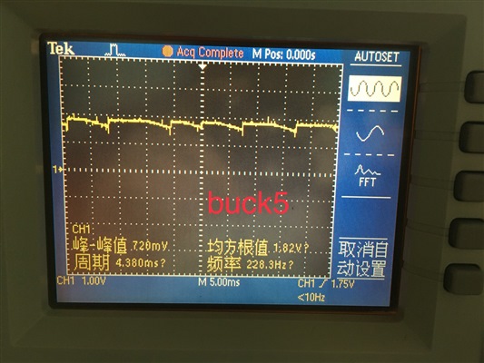
    One more question: the buck5 output ripple is huge(sorry for no scope shot and we just talk about it:) )and the average value is about 1.6V, and the SW1 and SW2 give 1.0V output, which should be 1.8V. The ripple on buck5 can affect the SW1 and SW2 seriously? 

    Thanks again

    Chunjie

  • Hi Chunjie,

    Thank you for checking the FET soldering. CSD87331Q3D is a great choice for making manufacturing easier.

    For output ripple on BUCK5 - it looks like per schematic there is only 1x10uF capacitor? We recommend minimum of 22 uF. Increasing that should help. For final board, I would also recommend connecting the FB point to the capacitor. There will be some ripple on the FB pin right now due to the parasitic RL of the via to the output cap.

    I do not understand what you mean by SW1 and SW2 are 1.0V output. Those are switching pins, they don't have a DC output. I would note again that if any voltage regulator is failing, the PMIC will perform emergency shutdown and then try to power up again if you keep the enable pin high. It is very common for customers to think that outputs are measuring low DC values because of this (on at correct voltage for x time, off for y time leads to measured value of correct voltage * (x/(x+y)).

  • Hi  Kavin,

    Sorry for the TYPO. It is SWB1 and SWB2, not SW1 and SW2. The capacitor has been increased on BUCK5 and the quality is improved. Hava a doubt that SWB1 and SWB2 1.0V output is relative to the bad quality of BUCK5 output?

    Thanks 

    Chunjie

  • Hi Chunjie,

    I think I would need scope shots of PVINSWB1_B2 input and SWB1 output on the same scope shot. I didn't cover above but I don't see a major risk of having SWB1 and SWB2 merged on board even though they are not set to merged. The pull-down resistor of SWB2 will be enabled, so we would recommend enabling SWB2 by I2C after the power up sequence is complete to minimize power loss, or better yet just physically cut the SWB2 trace on top layer with a scalpel to disconnect it from the net.

    Are SWA, BUCK6, VTT LDO, and LDOA1 working as expected?

  • Hi Kevin,

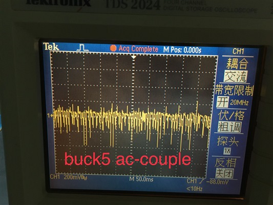
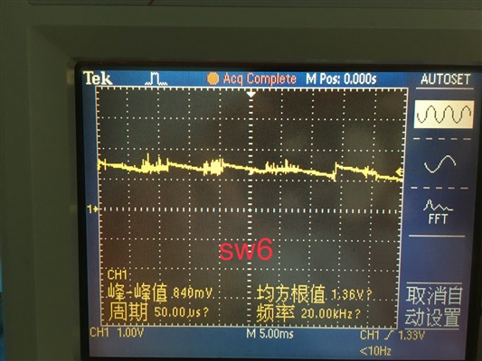
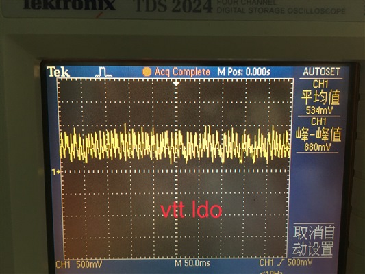
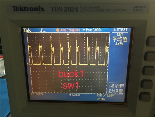
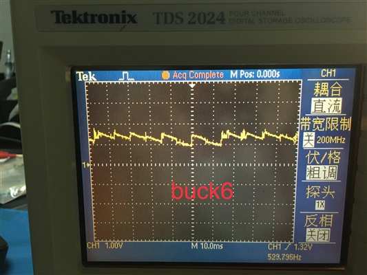
    To some extent, maybe we could say SWA, BUCK6, VTT LDO, and LDOA1 work but the quality is so bad with huge ripples, The scope shots are as attached.

    SWB1 and SWB2 are shorted in the pin, so it cannot be cut off. Only got one scope shot.

    PVINSWB1_B2 input is from buck5.

    We try to reduce the ripples by increasing the capacitance, however, the effect is minimal. Could you give me some advice to improve the quality? 

    As we know, the 2-layer stack-up is not friendly to power integrity. Under such a case, try to improve it as much as possible. As a freshman to the PMIC, we hope to get some debug experience ahead in order for our final product.

    Thank you 

    Chunjie

  • Hi Chunjie,

    From the BUCK5 scope shot, I do not see a no ripple issue. However there is still a power fault occurring on one of the regulators. You can see that it has about a 10 ms section where it is stable and then it shuts down before restarting. This suggests we should move to the next rail in the sequence.

    BUCK6 behavior is a bit confusing, I'm assuming this is the output, not the switch node. It looks like it is overshooting a bit during the initial turn-on; could be due to a variety of things on this board. FB routed parallel to switch node, FB connected closer to the inductor than the output caps, output caps only have 2 vias, current limit too low / not sensing properly, etc. But, it does stabilize at least once.

    Have you added an output capacitor to LDOA1 already? It is the last regulator in the sequence and it will not be stable and will power fault if you have not added a capacitor to the output.

  • Hi Kevin,

    During the debug, it is found that both BUCK5 and BUCK6 work on and off, and the time interval is about 10ms. 

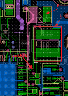
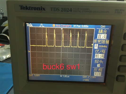
    From the PCB layout, BUCK6 SW is close to the inductor and the distance is only 20mil, which I think is close. Now there is no load on BUCK6, the two vias on output cap can affect the output? This time, both the output scope shot and SW scope shot are provided, which may give you some hints, I hope.

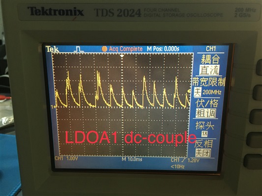
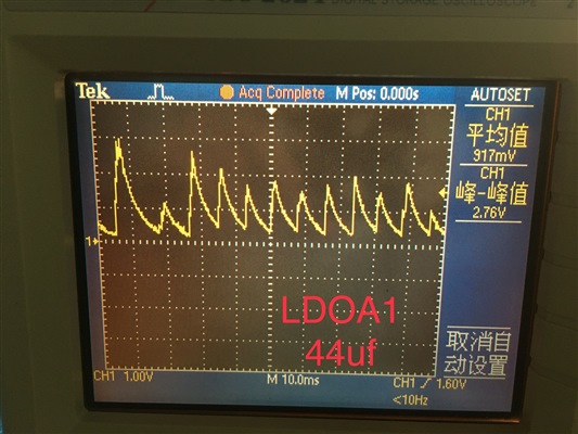
    For the LDOA1, a 22uf cap is added, and the scope shot is labeled as LDOA1 dc-couple and 2 22uf caps are also added, and the scope shot is labeled as LDOA1 44uf. 

    Based on the output of LDOA1, it seems not to work, which leads to the BUCK5 and BUCK6 on and off, right?

    Regards,

    Chunjie


  • Hi Chunjie,

    The SW1 images are too low of resolution to really be confident on what it looks like, but there appears to be a dip in the middle. This might indicate that the input power to the buck regulators is potentially failing. PMIC could shut off due to a UVLO event.

    LDOA1 behavior is unexpected. It almost looks like it tries to turn on at about the same time the PMIC is starting an emergency shutdown. It may be related or it may not. 

    Are you able to read the I2C registers? They would tell you which fault is being triggered. You can use a USB2ANY with the IPG-UI to read from the device after one of the resets. If you can keep the enable pin low then you should be able to try to start, keep it low, and read out which regulators are failing.

  • Hi Kevin

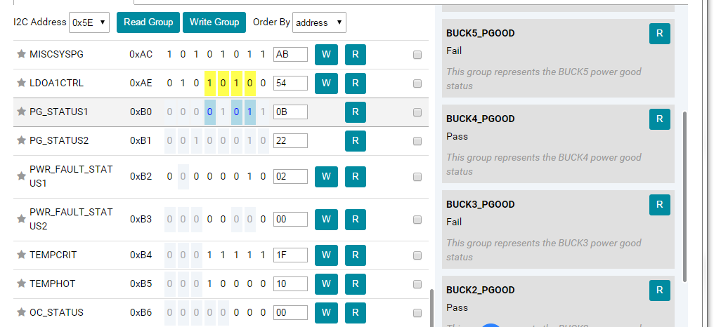
    We got a USB2ANY and readout all registers from the IPMC when it is enabled. The project JSON file is uploaded, which you could open with the IPG-UI, I think. If not, please let me know.

    From the power-up sequence, it is found that the BUCK3 fails first and there is a UVLO event in the registers. And it also says that the die temperature is high, but the actual temperature is okay, not hot.

    Thanks

  • Hi Chunjie,

    Thank you for providing the I2C readout. It looks like you still have CTL3 pin high. I would recommend taking the measurement after you force the CTL3 pin low, otherwise read is unreliable (PMIC is reloading OTP every time there is a power fault so read can be unreliable if taken during a power fault).

    UVLO is always generated on first power up, so it must be cleared to be meaningfu. It is always set on first power up since the previous shut off must have been from loss of power. So that is expected. CRITTEMP is occasionally set when there is a VSYS droop (digital becomes unstable as VSYS crashes) so we generally ignore it if the UVLO is still occurring.

    To check for UVLO issue, please power the board up with all CTL pins low. Then clear the UVLO bit and try setting the CTL3 pin high and see if it is still present.

    Looking at PWR_FAULT_STATUS1, we can see BUCK2 is power faulting. I think we discussed previously that the input capacitors for it are non-ideal. You could try taking scope shot of BUCK2 output and the voltage measured on R1284 to see how the voltage going into the FET looks during power up. Adding some capacitors closer to the FET may help.

  • Hi Kevin,

    The pictures in the previous reply are taken when CTL3 is high indeed. 

    I'm kind of confused about taking the measurement after forcing the CTL3 pin low. As known, when CTL3 is low, the PMIC enters to reset state. Do you mean taking the measurement when keeping CTL3 low? Or take the measure when CTL3 is switched from low to high?

    Thanks

    Chunjie

  • Hi Chunjie,

    PMIC does not enter a reset state when CTL3 is low. CTL3 being low just disables the regulators who use the CTL3 as par of their enable tree.

    I just mean reading the registers when CTL3 is low.