This thread has been locked.

If you have a related question, please click the "Ask a related question" button in the top right corner. The newly created question will be automatically linked to this question.

TPS2663: TPS2663

Part Number: TPS2663

Dear All,

we would like to use the E-Fuse TPS26633 to control the inrush current of the powert supply (Cout). The device is a display, that needs about 0,8A nominal current at 24V. The inrush current can reach 25A during the start up.  We would like to limit it at about 4.5 to 5A. I have tried to calculate the capacitor value and the rising time of the voltage (see below. Texts are in German but you can just understand the equations) for these both current values.

My issue is that, after checking the caculation excel sheet provided by TI, it is not possible to set the value of the inrush current higher than 3A. (inrush +nominal current). It is also not possible in this sheet to set an inrush current higher than the nominal current.  The sheet with my set values is also attached. 

Is it possible to simulate the circuit withits model? 

Thank you in advance 

looking forward to replying 

Best regards

Gilbert

is  can reach 25A during the start up.  We would like to limit it at about 4.5 to 5A.

Beispielrechung :  Inrusch Current = 3A und 5A

Der Inrush current can laut Datenblatt mit einem Kondensator am dVdT Pin begrenzt werden. 


Berechnung der Anstiegszeit der Spannung:

I(inrush) = C(out) * Vin/ tdVdT

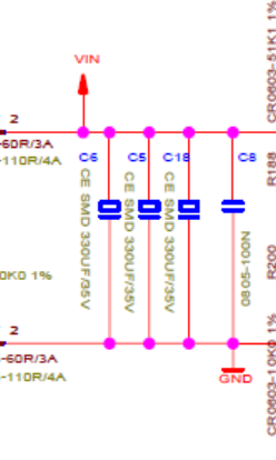
dabei ist C(out) die Gesamtkapazität am Ausgang vom E-Fuse. in unserem Fall C5, C6, C18. 
Vin ist die Eingangsspannung vom E-Fuse. In diesem Beispiel : 24V
tdVdT ist die Anstiegszeit der Spannung am Kondensator. Die ist die gesuchte Unbekannte.


=> tdVdT = C(out) * Vin / I(inrush)  =  (330uF * 3 * 24V) /3A  = 7,92ms
                                                                                                                                     
    tdVdT = C(out) * Vin / I(inrush)  =  (330uF * 3 * 24V) /5A  =4.752ms


Brechnung der Kapazität für die oben angegeben Anstiegszeiten:

Mit dieser zweiten Formel kann anhand der ermittelten Anstiegszeit der Wert des Kondensators berechnet werden : 

C(dVdT) = t(dVdT) /20,8*10^3 * Vin 

hierbei sind:
C(dVdT) :  die gesuchte Kapazität

20,8*10^3  : von Hersteller angegebenen Wert

Für I(inrush) =3A
C(dVdT) = 7,92ms /20,8 *10^3 * Vin = 15,86 nF
 
Für I(inrush) =5A
C(dVdT) =  4.752ms /20,8 *10^3 * Vin = 9,15nF 

  • Hi Gilbert,

    Welcome to E2E!

    Unfortunately, the attachments are not working. Can you please attach the sheets again. 

    Best Regards, Rakesh

  • Hello Rakesh,

    thank you for replying. I do not know why the attachment is not working. Is there any special way to attach the file?   But what about my description? I just want to control the inrush current using the TPS26633 IC and the actual value of this insrush current is about 25A. Is it possible with the TPS26633 to regulate it at about 4.5 to 5A. is ti possible ? The the power condensators i would like to charge are 3 x 330UF. Is it possible to set the Inrush current higher than the nominal current of de device? 

    On thwe link below you will find the calculation tools further down on the page as well as the simulation model. But i do not know how to use this model too. 

    Please check and let me know 

    BR

    Gilbert

    https://www.ti.com/product/TPS2663?keyMatch=TPS26633%20CALCULATION%20TOOL&tisearch=Search-EN-everything&usecase=part-number#design-development

     TPS2663x _TPS1663x_Design_Calculator_revB.xlsx

  • Hi Gilbert,

    The design sheet follows different calculation approach. 

    Getting back to your hand calculations.. Do you have target startup time ? else lower inrush current with large Cdvdt capacitor (47nF or 100nF)  helps reduce stress on the device.

    The device output current during startup will be the minimum value of the current limit setting and the inrush current setting. So, if you wish to continue with 3A inrush current, set current limit value above 3A. 

    Do you have EVM at your hand for evaluation? 

    Best Regards, Rakesh

  • Hello Rakesh,

    Thank you for your replying.  I do not really have any defined startup time. I have tried to calculate the inrush current based on 47nF Capacitor. I can get a startup ime of about 24ms with an Inrish current of about 1A ( See the calculation below).

    I do not really understand if you say: 

    "The device output current during startup will be the minimum value of the current limit setting and the inrush current setting. "

    Do you mean Iinrusch + Ilim = device output current ? 

    I have  placed order for this avaluation Board : https://www.ti.com/tool/TPS26630-33EVM. But I also wanted to know, how to use the simulation model. 

    Thank you in advance 

    Best regards 

    Gilbert

    tdVdT = C(dVdT) * 20,8 *10^3 * Vin =  47nF * 20,8 *10^3 * 24V = 23,4ms

    Berechnung vom Inrush Current mit 47nF : 

    I(inrush) = C(out) * Vin/ tdVdT  = 3*330uF * 24V /23,4ms  = 1A. 

  • Hi Gilbert,

    I mean the device output current  = min ( inrush current set due to dvdt cap , current limit setting).

    For example here, the inrush current is 1A with 47nF dvdt capacitor. If the current limit is set to 0.5A then the device output current will be 0.5A only.

    Please use the attached PSpice model for simulations 

    SLVMD03.ZIP

    Best Regards, Rakesh

  • Hi Gilbert,

    Please let me know if there are any further questions on this.

    Best Regards, Rakesh

  • Hello Rakesh,

    Thank you for your last Email. Sorrry for my late answer, I was little busy meanwhile. I still have some questions regarding the Chip TPS26633. 

    You spoke last time about the  the capacitor range to use on the dVdt pin (47nF ...100nF). So that means, the maximum Inrush currrent can only be about 1A as I caculated last time. What about if my device nominal current ist set at 2A for example?  doesn't I need to consider the device nominal current if calculating the Inrush current?

    In the caculation sheet, I also do not understand why the device nominal current cannot be less than the Inrush current. 

    What about the surge behavior. We are also scare about that the device can limit the surges and ESD pulses applied on the on it according to the EMC reqirements. I mean due to Ilim setting.

    If I chose for example an Inrush corrent based on 100nF Capacitor (about 470mA) is there any issue if my device nominal current ist still set at 2A ? of course Ilim can be set higher.

    Is the only disadvantage the start up time in this case?

    My idea with the chip is to use the PGOOD output to switch off first the DCDC coverter , when charging the 3*330uF Capacitors and switch on after. So in this case i do not need to consider the device nominal current. What do ou think about it? 

    Please let me know

    BRGilbert

  • Hi Gilbert,

    Sorry for the confusion on the design sheet. We may need to rework to make it simple..  The inrush current and the normal operating current are independent. 

    If I chose for example an Inrush corrent based on 100nF Capacitor (about 470mA) is there any issue if my device nominal current ist still set at 2A ? of course Ilim can be set higher.

    No.

    Is the only disadvantage the start up time in this case?

    Yes, longer startup time due to 100nF capacitor 

    What about the surge behavior. We are also scare about that the device can limit the surges and ESD pulses applied on the on it according to the EMC reqirements. I mean due to Ilim setting.

    During surge event, the device fast-trips the path due to large currents generated by the surge transient voltages.. but the device recovers quickly and resumes operation in current limit mode. Hence, the recovery time depends on the current limit set point. 

    My idea with the chip is to use the PGOOD output to switch off first the DCDC coverter , when charging the 3*330uF Capacitors and switch on after. So in this case i do not need to consider the device nominal current. What do ou think about it? 

    Yes, you don't need to consider device nominal current as the downstream load (DC-DC converter) is enabled using PGOOD signal of the eFuse.

    Best Regards, Rakesh

  • Hi Rakesh,

    Thank you for your last reply. 

    You said the chip will clamp the surge transient voltages applied on the device input Path. Are these transients not going to stress or damage the chip?  What about the overvolatage limiting feature when applyiing some Does also the overvoltage limiting feature reacts to the EMC surge transient? Is it possible to provide any measurements regarding these issues ( reaction of Current and overvoltage limiting features due to surge transients applied on it).

    I would also like to understand the working principle of the chip to let the output voltage rise up  gradually. is there any basic schematic to explain it? 

    I could not integrate the simulation model to my design. Is it possible to help for that goal? (only if it is easy for you)

    Please let me know

    BR

    Gilbert

  • Hi Gilbert,

    The device suppress the transient voltages reaching the load as long as the input transient voltages are with the recommended voltage rating of the device. For surge kind of events, an input TVS is needed to clamp and shunt the large surge current. The test waveforms Figure-50 & 51 in the datasheet shows the surge response during 500V/2Ohm surge.

    Sorry. Unfortunately, we can't share the internal functionality of the device. 

    Best Regards, Rakesh