This thread has been locked.

If you have a related question, please click the "Ask a related question" button in the top right corner. The newly created question will be automatically linked to this question.

TPS7A47: can it handle pulse load current?

Genius 3870 points
Part Number: TPS7A47

Hi there,

we are considering use TPS7a4701 as tracking LDO in this thread (

), some questions to consult.

Vin = 14.4V(battery) or 19V(adaptor),  Vout = Vin-0.3V.

Question1:  For its current limit behavior : suppose during test we intentionally set a large CONSTANT I_load of 5A, we would see the I_out be limited to 1.26A(typical) according to section 7.3.1 in datasheet, and I assume the Vout will drop drastically. As time pass,  4701 will became hotter and finnally trigger its thermal shutdown. After shutdown it will become cooler, and when temp cools down below 150°C, it will work again but still in overload situation if 5A load is still ON. As this cycle goes on, the device will eventually damaged because of overheat. Is this perception correct ? 

Question2: The load current is not constant vaule but intermittent pulse wave.  average current is less than 1A , but the peak transient current could be as high as 4.5~5A . 

From pic1, you can see in 150ms peorid there is 125ms I_load = 0 and 25 ms I_load is rippling as pic 2(zoom in) shows, the ripple cycle in every 25ms is about 12us and nearly 5A. 

I am concerned and not sure whether 4701 would be able to respond in time? or how fast (how short the current spike lasts) could 4901 response?  We will have to test on board, but it would be better if TI has relevant data or info to reference. 

Pic1. Current waveform Channel4 

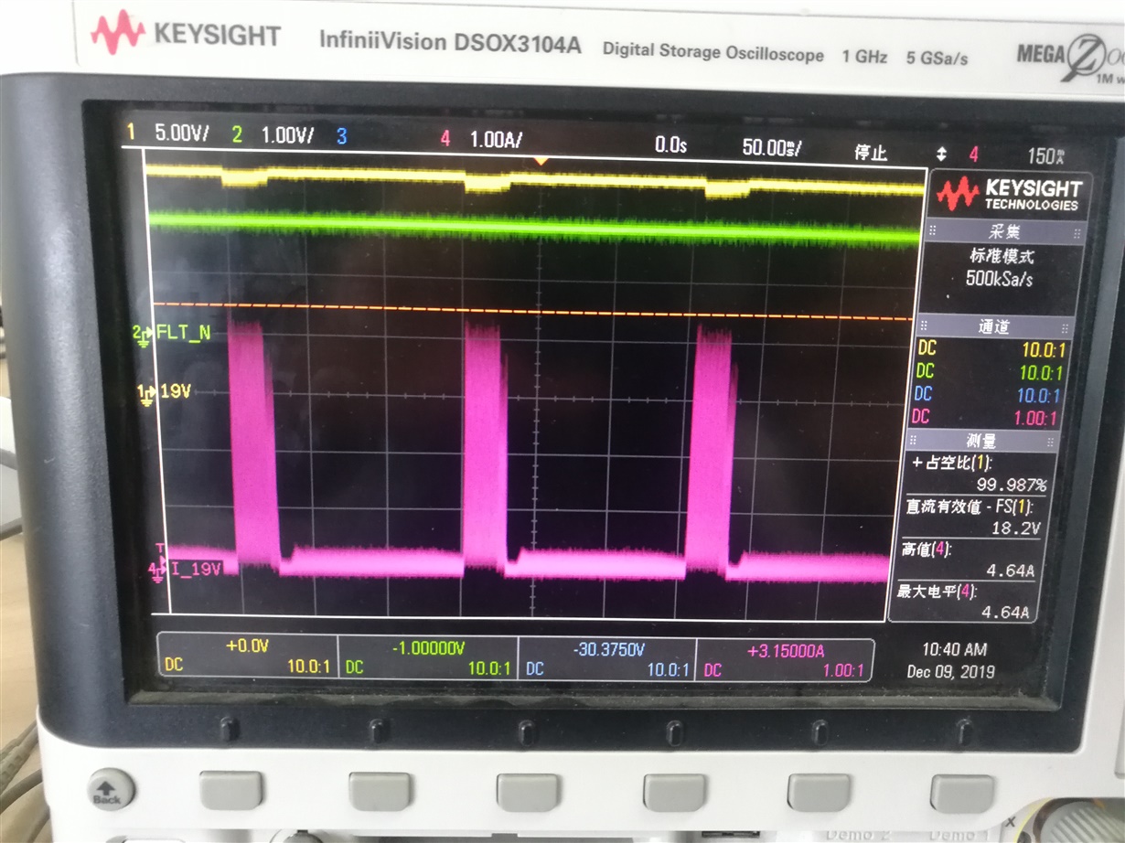
Pic2. zoomed in waveform (more details)

Thanks !!

  • Hello Yi,

    First, what you need will not be a simple linear regulator with only an input cap and output cap.
    This type of application requires additional components to work.

    Second, it sounds like you need a fast current limit.
    In general, thermal time constants are on the order of milliseconds, so a very fast current pulse before the current limit is engaged is not likely to heat up the component by a lot.  Unless you are operating right up against the maximum junction temperature, this probably wouldn't be your main issue.  However the internal bond wires can be fused at some significant amount of current.  That will be our main concern, if your pulse amplitude is high enough.

    Having said that, based on my experience when a pulsed load appears, the power converter (here, an LDO) needs to regulate current and not voltage.
    So your output should become a current regulator and not a voltage regulator while the load is pulsing.
    Then once the output achieves the desired steady state voltage, it should regulate the voltage and not current.

    During the time when your linear regulator is regulating current, you can tolerate droop on the output.
    This is because you are current limiting at something like an amp, but the load is taking something like 5A.
    Based on how much droop you can tolerate, will set the requirement for the amount of output capacitance.
    The good news is that the TPS7A47 is very stable and only needs a minimum load cap of 10uF for stability.

    Perhaps the hardest part is going to be maintaining a small voltage drop from the input to the output, but I have some ideas for that as well.

    As for thermal, RθJA of this device is 32.5 C/W.  Let's say we maintain 0.5V of headroom and current limit at 1A.  Then our maximum temperature rise is 17C and the reliability of the component will not be compromised for operation at room temperature.

    Please let me know if I've understood your requirements correctly.

    Thanks,

    - Stephen

  • Hi Stephen, thanks for you detail reply.

    let me explain more clearly ,and you can also get more infomation from the  original post. 【https://e2e.ti.com/support/power-management/f/196/p/899171/3340710

    As I wrote and discussed with your colleague John Cummings in the original post, our requirements can be summarized as :

    1. Vout= Vin-0.3V(or so). tracking function can be realized by overriding NR pin to turn it into a tracking LDO as John suggested.

    2. PSRR high, >40db at 800khz, that why we considering TPS7A4701.

    3. Able to provide the pulse current load as the 2 pics I attached above.  my concern is how will 4701 act  (or performance degraded) to this load, I do not really need a fast current limit, maybe I should not use the word "handle" but should use "provide".

    For my Question1, as I read in datasheet section 10.3, I think my understanding is correct that under CONSTANT over current condition the chip will cycles on and off automatically.

    And for my Question 2,  from the info you provide, I guess 4701's thermal protection circuit will NOT be able to response timely to this kind of fast pulse current load so its junction temperature is not like to rise up in a short time. However, the bonding wires may be fused if this current is too high (near 5A)  as you mentioned. This is the actually what i am concerning.

    May be the best and final solution is to find some IC that can actually provide 5A current, or build LDO with discrete components (mosfet and amp) as we used to do in the original post , but the PSRR will always be a tough target to achieve. 

    PS :  Quote you words "Perhaps the hardest part is going to be maintaining a small voltage drop from the input to the output, but I have some ideas for that as well.". I would like to learn your insignt on this, too.

    Thank you again!

  • Hello Yi,

    Let me clarify that for a single, fast pulse, the thermal junction temperature of the die will probably not increase significantly.
    For many pulses in a short period of time, this can look like a longer pulse from a thermal perspective and that might raise the junction temperature.
    However if we keep the headroom to a small value, the overall junction temperature rise will be manageable as long as the ambient temperature is not too high.

    The design method that John provided might be worth trying first.
    My concept would be to use a dual setpoint design, but it has a few more components than John's NR pin based solution, so I think testing that concept on an EVM first would be a good idea.

    We do not recommend operating in an area where protection circuits take over, such as thermal or current limit.
    It is difficult to give a quantifiable answer on how the reliability of the component is affected, as everyone's circuitry and operating conditions are different so producing this data is not feasible.  You may wish to add a secondary LC filter on the output of the LDO to help squash the peak current of the load pulses. 

    When the linear regulator enters current limit, the output will droop for the remainder of the pulsed load.
    How much can your system withstand a drop in output voltage during a pulsed load event?

    Are you certain that 5A peak is the maximum amplitude pulse the load will see?
    What is your fastest rise time and fall time of the load pulse?

    Do you need the PSRR during current limit?
    PSRR as shown in the plots is largely a function of the voltage loop gain.
    But when the current limit protection circuit takes over, the voltage loop is no longer in control.
    I would expect that the PSRR would change quite a bit in current limit.
    We would need to add some external components to force the LDO to regulate current and not voltage during a pulsed load, if you need the PSRR during current limit.

    Thanks,

    - Stephen

  • Hi Stephen, to answer your questions:

    How much can your system withstand a drop in output voltage during a pulsed load event?

    ----------I checked with our SE, it is hard to accurately define the acceptable dip on Vout, about 5% should be use. that is 19V*0.05 = 0.95V or 14.4V*0.05=0.72V

    Are you certain that 5A peak is the maximum amplitude pulse the load will see?

    -----------almost certain, there are tens of working mode of our machine, these pics are nearly the highest current we watched until now.

    What is your fastest rise time and fall time of the load pulse?

    -----------also this is hard to answer, as there are tens of loads , but it should be around 5us or so. May I ask why you care about this parameter? thanks.

    Do you need the PSRR during current limit?

    -------we need it. actually our SE hope the current limit not happen. this requirement might largely limit us using high performance off-the-shell LDO like 4701. but we would test  on bench first. 

    by the way, I am not sure I understand your idea  that "My concept would be to use a dual setpoint design" in design a tracking LDO ? I would like to learn .

    Thanks again!

  • Hi Yi,

    Thanks for the data.
    The rise and fall times are important because these will impact the current spike seen by the LDO, before it can enable the current limit (either internally or any external current limit circuit we design).  A very fast rise time means we have to design a faster circuit with a higher bandwidth, which is harder to do.
    We will use 5A for now as our maximum current amplitude and 5us for the rise and fall time.

    We do not characterize PSRR during current limit conditions so we do not have data to suggest how well this performance parameter works during this protection mode.  You can use the EVM to test the TPS7A47 to see if your needs are met in the system during current limit.  If your system performs well and meets requirements, we just need to review the bond wire current (I'll work on that and get back to you).

    Let's discuss the NR pin approach.  The "Noise Reduction" or NR pin is typically used to provide a very low pass filter for the reference voltage.  If you directly connect a bias source like Vin through a diode, you will be directly injecting any noise on the input into the error amplifier, which has high gain.  Without sufficient filtering on the NR pin, you will not achieve the 40dB of PSRR.  So with this approach, take care to filter out Vin with a low pass filter on the NR pin.

    If you find the NR pin approach insufficient due to this noise, you can switch to the dual setpoint approach.  This prevents noise on the input from reaching the internal error amplifier, but it requires more components.  A dual setpoint approach would detect the input voltage and change the setpoint on the output accordingly.  This method would require an additional comparator, a zener diode, a low signal mosfet and some additional passive components.  The setpoint resistors could be designed to be within whatever tolerance your system requires, such as Vin - 1V. 

    If possible we could use the ANY OUT connections to save a few external resistors.  Then the MOSFET would simply connect the necessary ANYOUT connections to ground, instead of Rbottom2.  Using external feedback resistors, a basic drawing would look something like this.

    Thanks,

    - Stephen