This thread has been locked.

If you have a related question, please click the "Ask a related question" button in the top right corner. The newly created question will be automatically linked to this question.

UCC28950: UCC28950 and UCC21520 circuits and sequences

Part Number: UCC28950
Other Parts Discussed in Thread: UCC21520, , UCC28951

Hi,

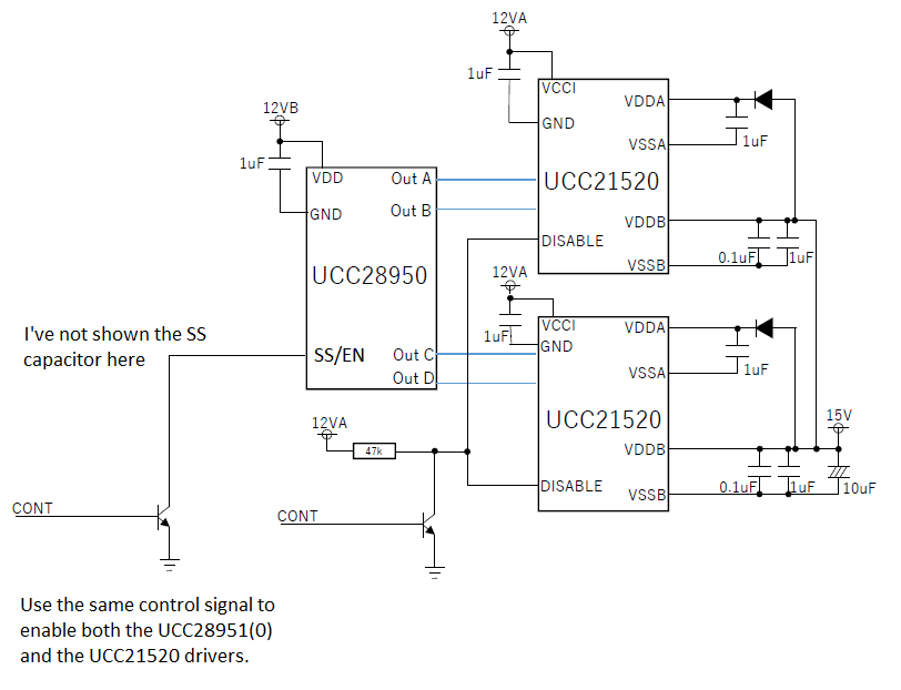
I'm considering a circuit using the UCC28950 and UCC21520 devices.
A schematic circuit and sequence are shown in the attached material.
I first thought of the PLAN1 circuit. However, due to the relationship with other circuits, VDD of UCC21520 is applied first.
Therefore, I am concerned that it may cause malfunction of the circuit.
Therefore, like PLAN2, I am considering adding a control circuit using Disable.
Is the PLAN2 circuit and sequence good?
In that case, should the UCC21520's Disable release timing be the timing when VDD of UCC28950 becomes 7.3V or more?

Best regards,UCC28950 and UCC21520 circuits and sequences.pdf

  • Hello

    First - I would suggest you use the UCC28951 instead of the UCC28950. The UCC28951 device is an enhanced version of the UCC28950. It is a fully compatible drop-in replacement for the UCC28950. Refer to application note SLUA853 at http://www.ti.com/lit/an/slua853/slua853.pdf for more details. The UCC28951 is typically the better choice, especially for applications where the system may have to operate simultaneously at a duty cycle> 90% and current limit.

    For the sequencing I'd suggest that you add a control transistor at the SS/EN pin of the UCC28951 and use that to enable the controller once the power rails are ready - see below. That will give you control over the point at which the controller starts to generate output signals - much better than asynchronously enabing the drivers and hoping that all four drives become active at the same time. You could use the same CONT signal - the UCC28951(0) will not generate any outputs until the SS/EN pin reaches 500mV - giving time for the CONT signal to enable the two UCC21520 devices.

    Finally - I'd suggest you use a small signal MOSFET to pull SS/EN down - the min SS?EN disable voltage is about 200mV and this is very marginal considering the max VceSat. A OSFET removes this concern completely.

    The OUTx signals from the UCC28951(0) are locked to 0V as VCC rises from 0V until the device starts switching so there is no danger of incorrect glitch inputs to the UCC21520.

    Regards

    Colin