This thread has been locked.

If you have a related question, please click the "Ask a related question" button in the top right corner. The newly created question will be automatically linked to this question.

TPS54A24: Digitally controlled Buck converter simulation

Part Number: TPS54A24

Hi,

I am currently designing a circuit that include a digitally controlled buck converter. The input voltage is 12V, and the desired output voltage should be set between 0.6V and 11V, with 10A of maximum out current.

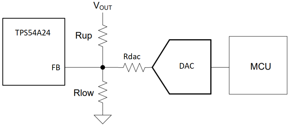
I am considering using the TPS54A24 with a DAC connected to its feedback network in order to set the output voltage. In order to evaluate the stability of the circuit in any condition I would like to perform some AC Analysis of the circuit, but I can only find the Transient spice model of the TPS54A24.

Is it possible to get an average or AC model of the TPS54A24 ? I also hear of a simulator called simplis that is pretty convenient for simulating switching power supplies. I can download it if needed.

Best regards,

Guillaume Levant

  • Hi Guillaume,

    It looks like we would need to request our modelling team to create an average model created for this part.

    How complicated is the circuit you would need to simulate? The attached excel sheet includes an AC model for this part. Maybe this is sufficient for your needs. Since you are varying the output voltage, you would want to be careful to make sure you input an equivalent feedback network for the different operating points you want to check.

    /cfs-file/__key/communityserver-discussions-components-files/196/PEAKCMC_5F00_BUCK_5F00_CALC_5F00_TOOL_5F00_191213.xlsx

    Let me know if the excel sheet works or else I can get the process started on getting an average model created.

    Anthony

  • Hi Anthony,

    I would like the typical application schematic, but with a DAC connected to the FB pin of the TPS54A24 through a resistor, this way :

    Thanks to this I would control the output voltage digitally. So regarding simulations I would like to do AC analysis for different values of the DAC output and different loads, so that I can make sure the circuit is stable in any condition.

    I don't know if the excel sheet could work for that application, given that the feedback resistors I would put would be different from the circuit I would design at the end, and I guess they would affect the frequency response.

    Best regards,

    Guillaume Levant

  • Hi Guillaume,

    You are right, this would affect the DC gain in the frequency response compared to the normal feedback divider. Specifically this is due to there being a different divide ratio than normal from the output voltage to the FB pin. The divide ratio would be fixed based on the maximum output voltage you need to support. For example for low output voltages, this DAC circuit would end up with more division from Vout to FB than a normal feedback divider.

    Luckily this excel sheet is set up in a way that it will work for your needs. In the Small Signal tab, put in the component values you would like to use. For Rhs FB and Rls FB specifically, put in your values for Rup and Rlow then ignore the DAC portion of the circuit. Rup for Rhs FB and Rlow||Rdac for Rls FB. With everything else fixed, you can just input different values for Vout to get their frequency response. In the image below I've circled in red the values which should be fixed based on the schematic and in green the values you would want to vary.

    The one thing you may need to change between the different output voltages is the capacitance of any ceramic output capacitors. Their effective capacitance will likely vary significantly depending on the DC bias. Especially with a range of 0.6V to 11V.

    One other comment which came to mind while looking at this again is to make sure you are aware of the limitation for the maximum output voltage. The maximum output voltage will be about Vin - Iout * (Rhs + Rdcr). With 12 V input, can get 11 V on the output at 10 A load as long as the DC resistance between the input and output is less than 100 mΩ. This doesn't account for any variation in the input voltage.

  • I made one correction to my last post. For Rls FB, put in the equivalent resistance of Rlow||Rdac.

  • Hi Anthony,

    Thank you for this information, I think I can use the excel sheet to cover all the cases.

    For the maximum output voltage formula, did you mean Vin - Iout (Rdson_hs + Rdcr) ? Because otherwise, Rhs being several kOhms, it is a pretty strict limitation :)

    Thank you for your help,

    Best regards,

    Guillaume Levant

  • Hi Guillaume,

    Right, I was referring to the Rdson_hs in that equation. I could probably be a little more consistent with variable naming :).

    Just let me know if you run into any issues with the excel.

    Anthony