


The DRV103 datasheet says regarding the PowerPAD: "Do NOT use the exposed metal pad as a power ground connection or erratic operation will result."
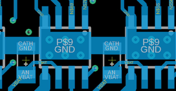
My design utilizes the copper under the PowerPAD to connect adjacent DRV103 chips to ground, but it has a wide trace connecting directly to the GND pin (pin 4) on each DRV103. Is this a problem? I have not noticed any erratic behavior, but I am unsure exactly how to interpret the datasheet. It *could* mean that if I left the GND pin disconnected and tried to rely on just the PowerPAD for chip grounding, then erratic behavior would occur. This implies that as long as I provide a proper power ground connection to the GND pin of the DRV103, it's fine to also connect the PowerPAD to this ground (this is what I've done). But it could also mean I should leave the PowerPAD completely isolated.
I've attached an image of my layout showing how an amply-wide connection is made to the GND pin (pin 4):
Any advice here would be appreciated.
Thanks!

