


Hi there,
Thanks for the help so far on the LMZM33606 I really appreciate the advice and support.
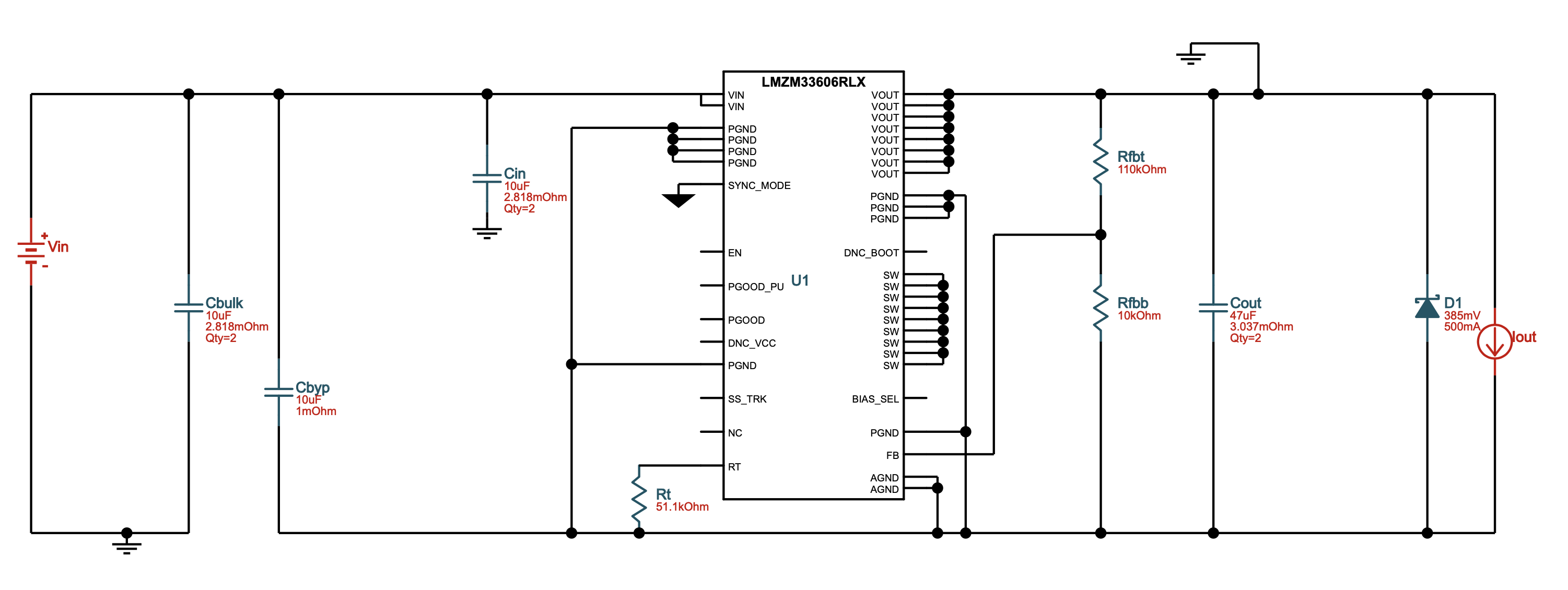
With regards to the IBB application of the LMZM33606 chip, the application notes don't include any suggestion for board layouts. My project requires the design to generate three rails 12V, -12V and 5V from two LMZM33606. My plan was to generate 12V from one chip and from that use a linear regulator to generate the 5V. For the -12V I was planning to adapt the 12V design as follows (for Vin 15-20V, generating max 3A):
Questions I have are:
1) Are there any layout guidelines for the additional components of Cbulk, Cbyp, D1? Or can I just follow the layout guidelines for the LMZM33606 and put these additional components anywhere? Should the same LMZM33606 guidelines for board layers and planes be followed for the IBB?
2) For the PGND in the diagram, can I connect those to the same PGND as the LMZM33606 circuit generating the +12V?
3) Is the SYNC_Mode in the diagram the only item connected to the AGND? Not sure if the black arrow means AGND or something else.
4) In Figure 1 of SNVA835B–July 2018–Revised May 2019, there is a SYS_GND in red. Where do I connect that to in relation to the overall design? Is it connected to the Vout plane that the +12V generating LMZM33606 is connected to?
5) All the power rails will come out of a 16 PIN connector. Should the rails be connected to the PIN outs using circuits on the top most layer?
6) The schematic diagram above is missing a CFF capacitor. Is a CFF required for the IBB application as per table 4 of SNVA835B (which shows values Cout = 435 uF and Cff = 100 pF)?
7) How much performance improvement in terms of lowering ripple and noise will be gained from clocking both LMZM33606 chips to the same clock? Is it possible to use the same clock given one of them is inverting its output?
Many thanks again for the support!
