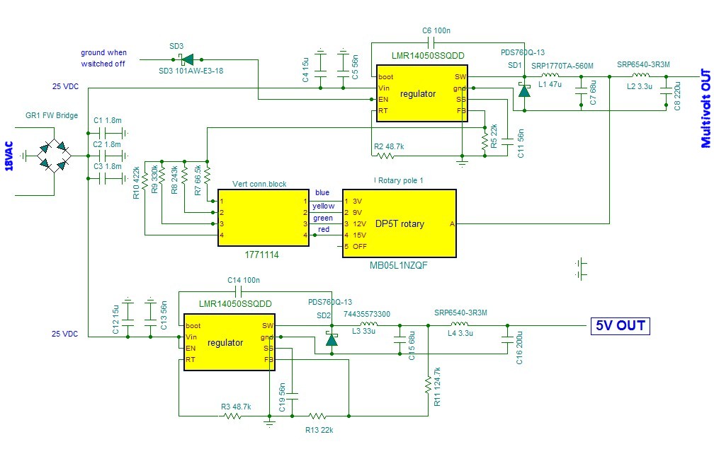
In response to suggestions in related questions I have decided to redesign the circuit and remake the board of LMR14050-based dual power supplies. If anyone feels up to it, I would appreciate any comments or further suggestions. The new schematic and layout is attached.
1) New component values for the two output stages: for the MultiVolt supply (switchable 15V, 12V, 9V, and 3V) the first stage inductor is 47uH and the output capacitor is 68uF ceramic. For the 5V supply the first stage inductor is 33uH and the capacitor is also 68uF. The inductors were sized using a 1.0A load (smaller loads require larger inductors) and K = 0.3.
The capacitors were sized with the datasheet criteria of under shoot and over shoot using I(oh) = 5A and I(ol) = 0.5A; V(os) = V(us) = 5% of V(out). Sizing for crossover frequency is reiterative with two stage outputs and shown later. From a nominal VDC (in) of 18xSQRT2 = 25.5 the actual V(in-average), accounting for the charge/discharge of the 5400uF bulk capacitance, is 20.15V with 5.0A load, and 23.25V with a 1.0A load. The second stage inductances and capacitances are 3.3uH (<0.1 of L-1) and 220uF (electrolytic) respectively. The inductor resistances are 22mR for the 33uH, 34mR for the 47uH, and 23mR for the 3.3uH. ESR is 0.0009R for the 68uFs and 6R for the 220uFs.
Considering both output stages, the effective first stage crossover frequencies are 1322Hz for the MV supply and 1556Hz for the 5V supply. The effective second stage crossover frequency is 12,156HZ for both supplies. The oscillator frequency is 500KHz. Output voltage ripple calculates as about 2.7mV for both supplies. The output current ripple calculates as 210mA(rms) for the MV and 200mA(rms) for the 5V supply. The input current ripple (rms) is too difficult for me to calculate with any precision. V(us) is within spec for both supplies; The MV V(os) is within spec, but V(os) is three times the spec limit for the 5V supply. As neither V(us) nor V(os) are a very critical operating spec for my application, they weren’t improved.
When compared with the WEBENCH design model, the component values and operation results are reasonably close ,when adjusted for oscillator frequency differences (WEBENCH uses 1.2MHz).
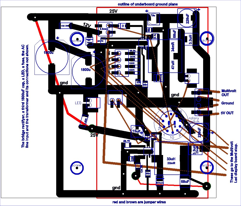
2) The largest material improvement is in the board layout and component placement. Earlier others have suggested such improvements but I was unable to physically accommodate them on the already made board. Plus it intuitively didn’t seem that critical. But now it seems to be the only solution to the current unresolved problem of output dropping to zero with any load greater than about 200mA. Both input capacitors, a 15uF electrolytic and a 56nF ceramic, are placed right next to the voltage input pins, almost atop for the ceramic. (These are fed from 5400uF bulk filter.) The output inductors and Schottky diodes are placed as close as physically possible to the SW output pins. The 1st stage output capacitors are place as close as possible to the inductor output. The 2nd stage inductors and capacitors are in close proximity to each other and the 1st stage components. The traces connecting the 1st stage and the 2nd stage output filters are as short and wide as possible. The voltage and ground traces are wide.
3) The FB connections and unfortunate wiring necessary for the switchable multivolt supply are as far from the inductors as possible. The FB resistors are as close to the FB pin as possible. The multivolt FB connecting wires are shielded with grounded conductive tape. All inductors are shielded wirewound. A ground plane of a double-sided board underlays the main circuitry with numerous VIAs connecting it. This plane also aids heat sinking.
Any thoughts? Any bets?