This thread has been locked.

If you have a related question, please click the "Ask a related question" button in the top right corner. The newly created question will be automatically linked to this question.

LM25141-Q1: LM25141 Vout not correct

Expert 1055 points
Part Number: LM25141-Q1
Other Parts Discussed in Thread: LM25141, LM5143

Hi,

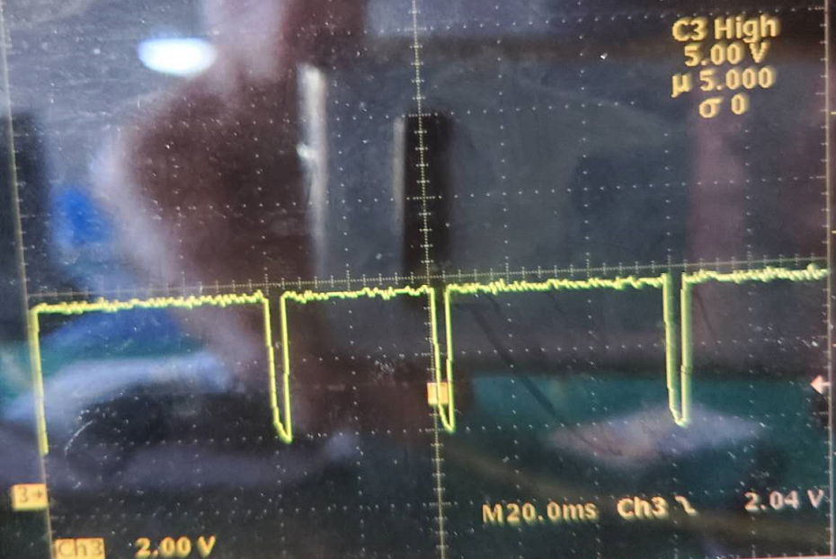
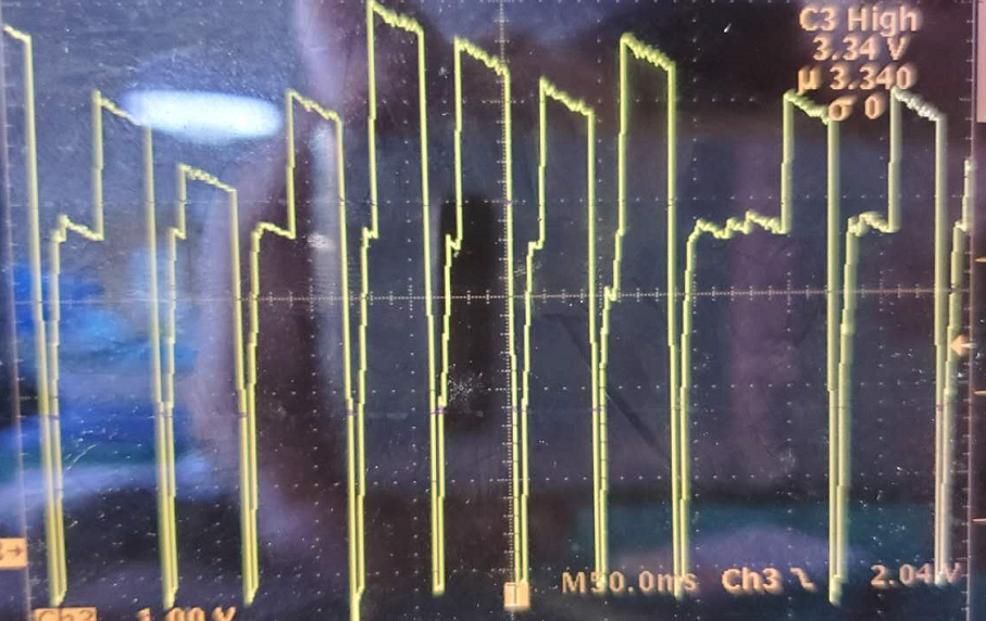
   Our own LM25141 PCB is setting work at 2.2.MHz switching frequency and 3.3V output,but i measure the VDDA & VCC are dropped about 2V(figure 1),also the Vout looks like unnormal (figure 2),could you point at what the problem for me?

  • Hi

    you can also check below:

    1. whether you use large Qg mosfet which make the VCC over current, you can connect a external votlage source to VCCX to proivde more current

    2. whether you have cermaic cap very close to VIN PIN of LM25141

    3. whehter your ANGD and PGND is connected right

    Thanks

  • Hi Daniel,

        1,I used the GaN FET,pls look at the parameters in figure below(first is HS and second isLS): 

        2,The Vin cap is close to the VIN PIN

        3,I use the 0Ohm resistor for connecting between AGND and PGND

  • Hi 

    have you tried external VCC and can you share the schematic and PCB layout?

    One thing you also can check is that you can disconnect the GanFET to see whether the  VCC and VDD is right. if it is OK, you may need check EN .

    GanFet has very high dv/dt which may easily interfere the chip's working statues, so it is very hard to predict which function has issue so that we may need schematic and PCB layout. 

    Thanks

    Daniel Li

  • Hi Daniel,

        When i disconnect the GanFET the VCC and VDDA are output 5V normally.

        Attached are the schematic diagram and PCB,the software is AD19

      IB PowerBoard.zip

  • Hi 

    For Ganfet application, recommend 4 layer PCB for better noise immunity.  and 2 layers layout is not good .

    1. As our datasheet suggested: Keep the high-current paths short, in your layout the CIN+->Q1->Q2->CIN- parth is too long especially Q2 GND->CIN GND which will have large inductance on the ground make the ground very noisy when Q1 turn on and off.

    2. your AND use R16 connect to PGND, but you choose a very noisy PGND around the Q2 Souce.

    3.the current sense trace routing is wrong, you should use Kelvin connection way

    I think you need a PCB change .

    Thanks

  • Hi Daniel ,

        Thanks for your advises.

        Another,if i want to change GaN FET into Si MOSFET,can you help me to confirm whether the MOSFET below can be drivered by the LM25141?

    ONSM-S-A0001842162-1.pdf

  • Hi 

    based on figure 8 of mosfet datasheet, at 5V, the Qg is 90nC, with 400Khz frequency, it need proivde 2*900nC*400Khz=720mA, which means the VCC need to proivde 720mA current to the driver.  it looks our internal LDO rdson is 2ohm it will cause 1.4V voltage drop from VCCx to VCC and include diode voltage drop, I think it maybe not enough to drive this mosfet.

    I suggest you use the two phase controller to drive high current , recommend LM5143

  • Hi Daniel,

       Can i understand that is the output voltage of HO & HOL are lower than 3V(≤5V-1.4V-0.6V=3V),so this MOSFET is not enough to conduct completely?

       But i can’t understand you said the drop voltage from VCCx to VCC,because the VCCx looks like unused ,in addition,why do you multiply 2 in the calculation of current which VCC provide?

  • HI

    using 2 means you have a pair of mosfet (high side and low side) , all the drive current provide by VCC.

    you have to use VCCX,cause without VCCX, internal LDO only can provide 75mA current(DS 7.3.2). 

    Thanks

  • Hi Daniel ,

       I'm so sorry that i still have a questions,as you said i must use VCCx ,do you mean increase the drive current through VCCx connect to external power?If it is,i think that can provide high current.

  • Hi

    Yes, You must use VCCx, but there is still internal impedance from VCCX to VCC as well as voltage drop on the boot diode. it is better to take look the Vgs voltage, it maybe has issue on the drive voltage.

    Thanks

  • OK,now i am totally clear,thanks for you