Hi TI,
I am currently using a 12V input adapter to charge a 4S1P LiFePo4 battery (maximum 14.6V). The charging chip BQ25703A works in Boost Mode. The bqstudio host computer register configuration is as follows:
Charge Option 0 820E
Charge Current Register 0800
Charge Voltage Register 3900
OTG Voltage Register 0000
OTG Current Register 0000
Input Voltage Register 2100
Minimum System Voltage 2D00
Input Current Register 3C00
Charge Status Register B400
Prochot Status Register 0040
Input Current Limit In Use 3C00
VBUS and PSYS Voltage Read Back 8410
Charge and Discharge Current Read Back 1E00
Input Current and CMPIN Voltage Read Back 3900
System and Battery Voltage Read Back B2B1
Manufacture ID and Device ID Read Back 7840
Device ID Read Back 1078
Charge Option 1 9210
Charge Option 2 02B7
Charge Option 3 0000
Prochot Option 0 4A54
Prochot Option 1 8128
ADC Option 2000
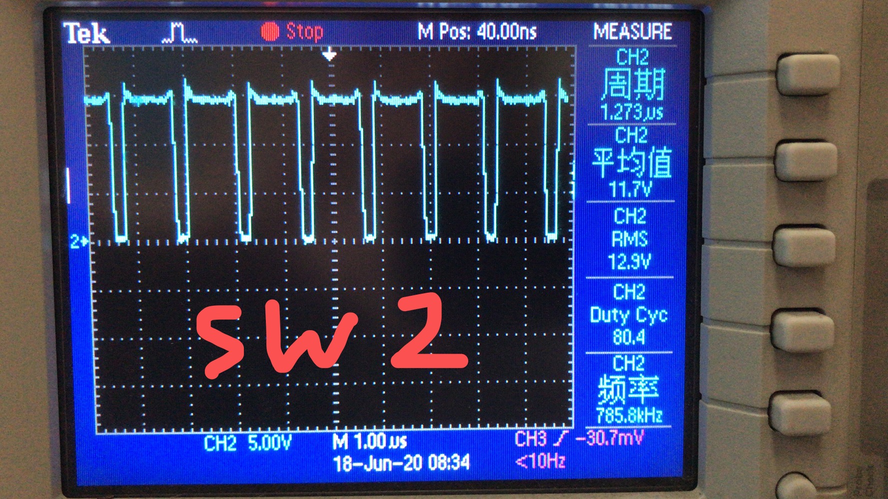
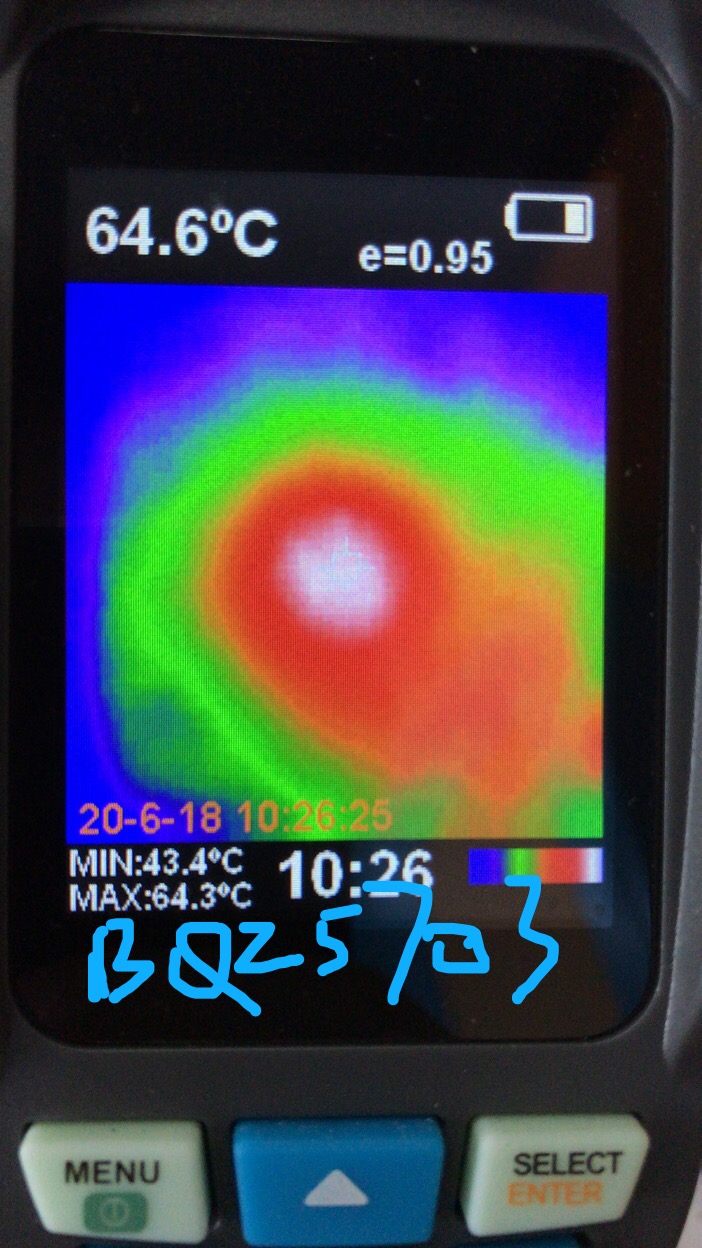
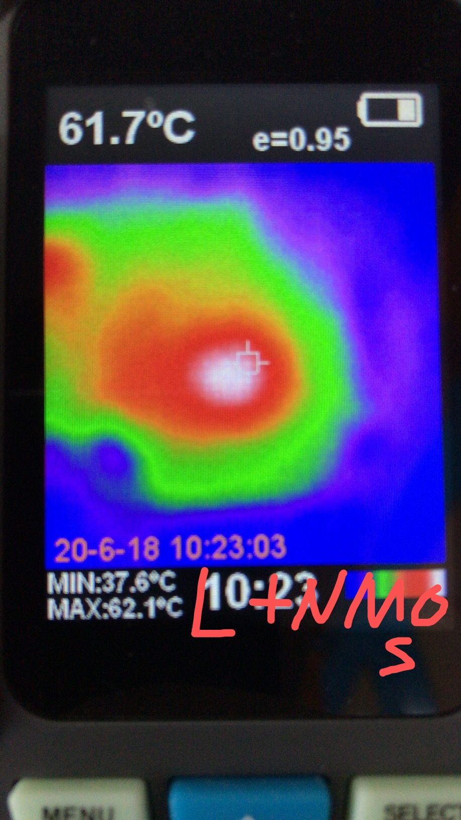
The above configuration : VIN=12V, VBUS=12V, VSYS&VBAT (the voltage slowly rises to 14.52V), the charging current is 2024mA, you will find that the inductance (L1) and two MOS tubes (Q14&Q16) and BQ25703A chip in the boost process of the charging process have a large amount of heat, The larger the charging current configuration is, the hotter it is, and there is no problem if the charging current is changed to 1024mA.
NMOS tube selects NTMFS4833NT3G, RDS(ON)= 2.0mR@10V, Id(max)=191A, SO-8 FL package;
Inductance: 74437356022 2.2 μH, 8.5 A, 0.0203ohm;
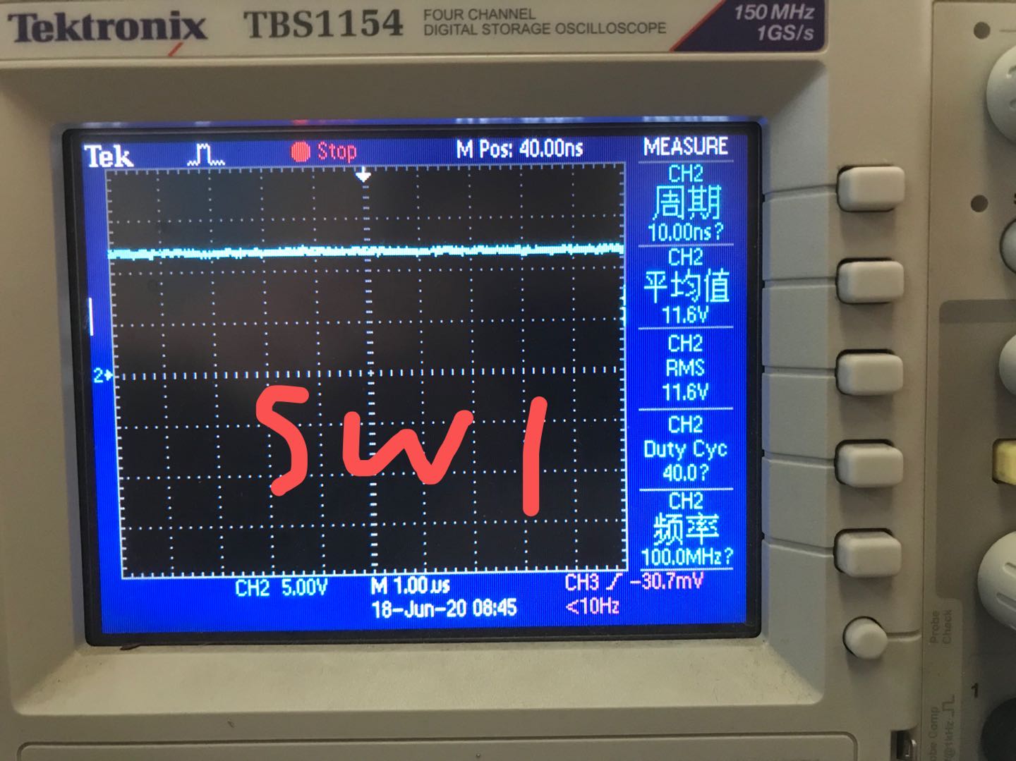
The following six pictures are SCH, PCB, signal waveform and heat map,
Is the above fever normal? How do the key signal waveforms compare? Any suggestions for PCB layout (need to increase heat dissipation area)?