This thread has been locked.

If you have a related question, please click the "Ask a related question" button in the top right corner. The newly created question will be automatically linked to this question.

TPS7A4501-SP: TPS7A4501: Output overshoot issues

Part Number: TPS7A4501-SP
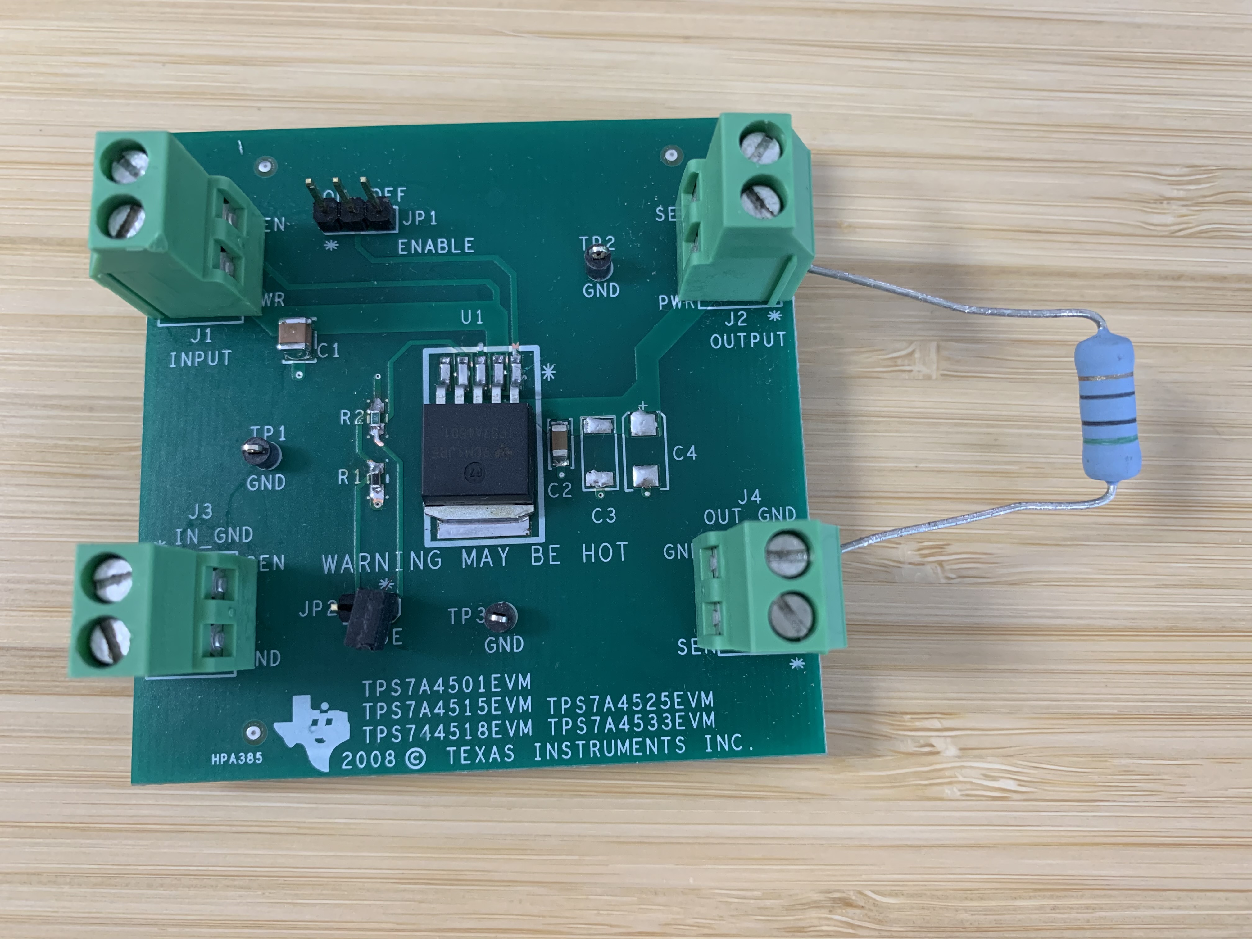
Other Parts Discussed in Thread: TPS7A4501EVM-385, TPS7A45, TPS7A47, TLV767

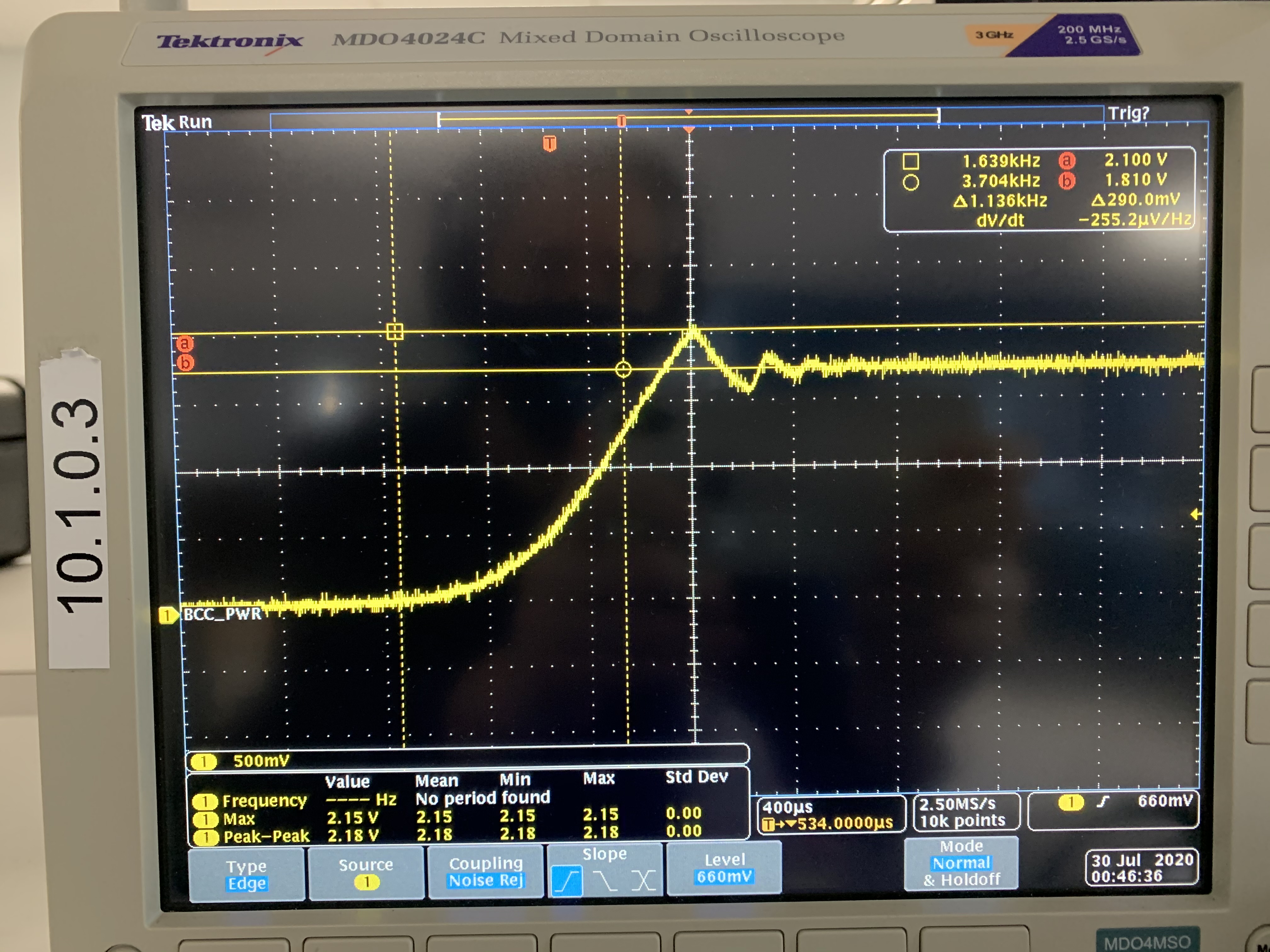
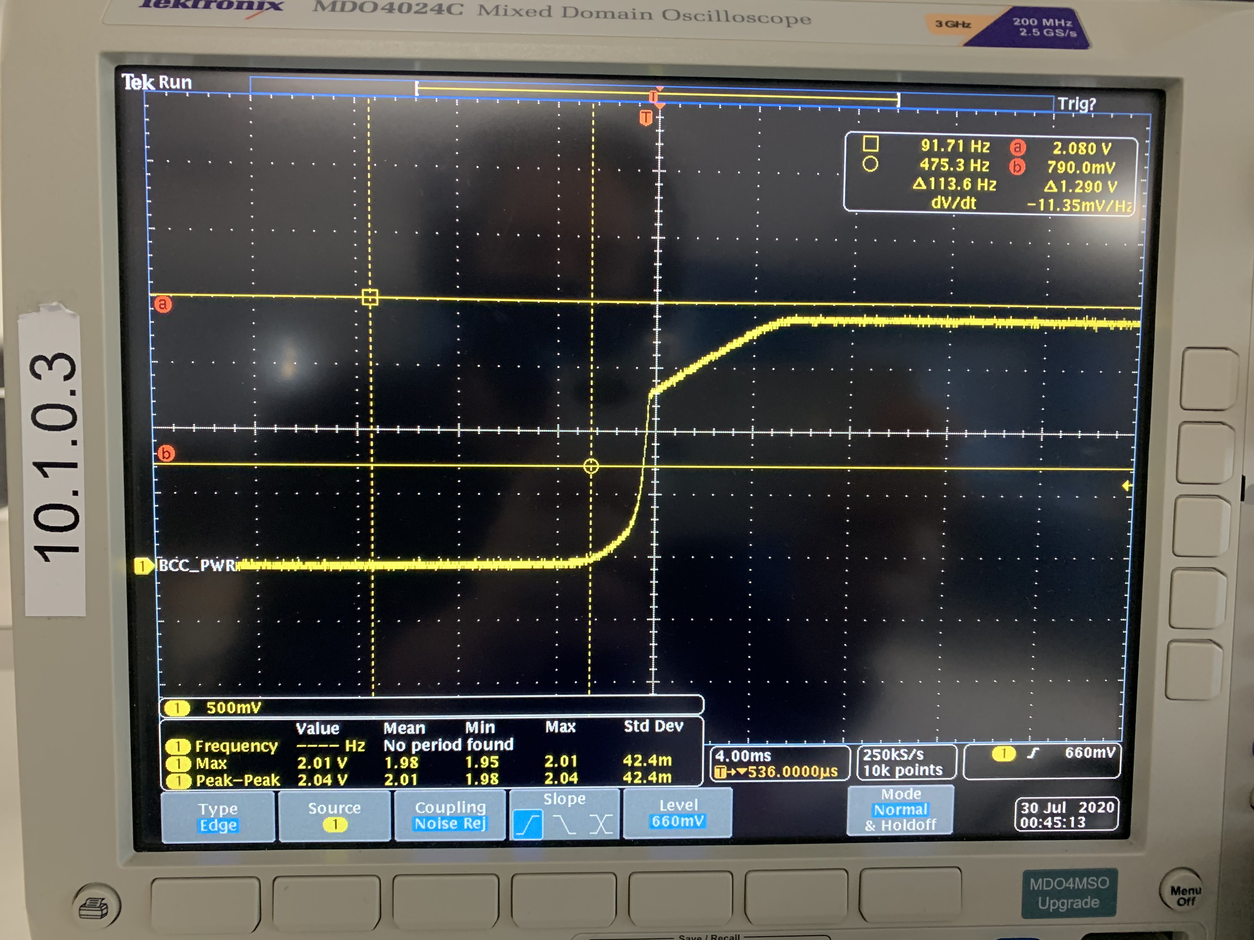
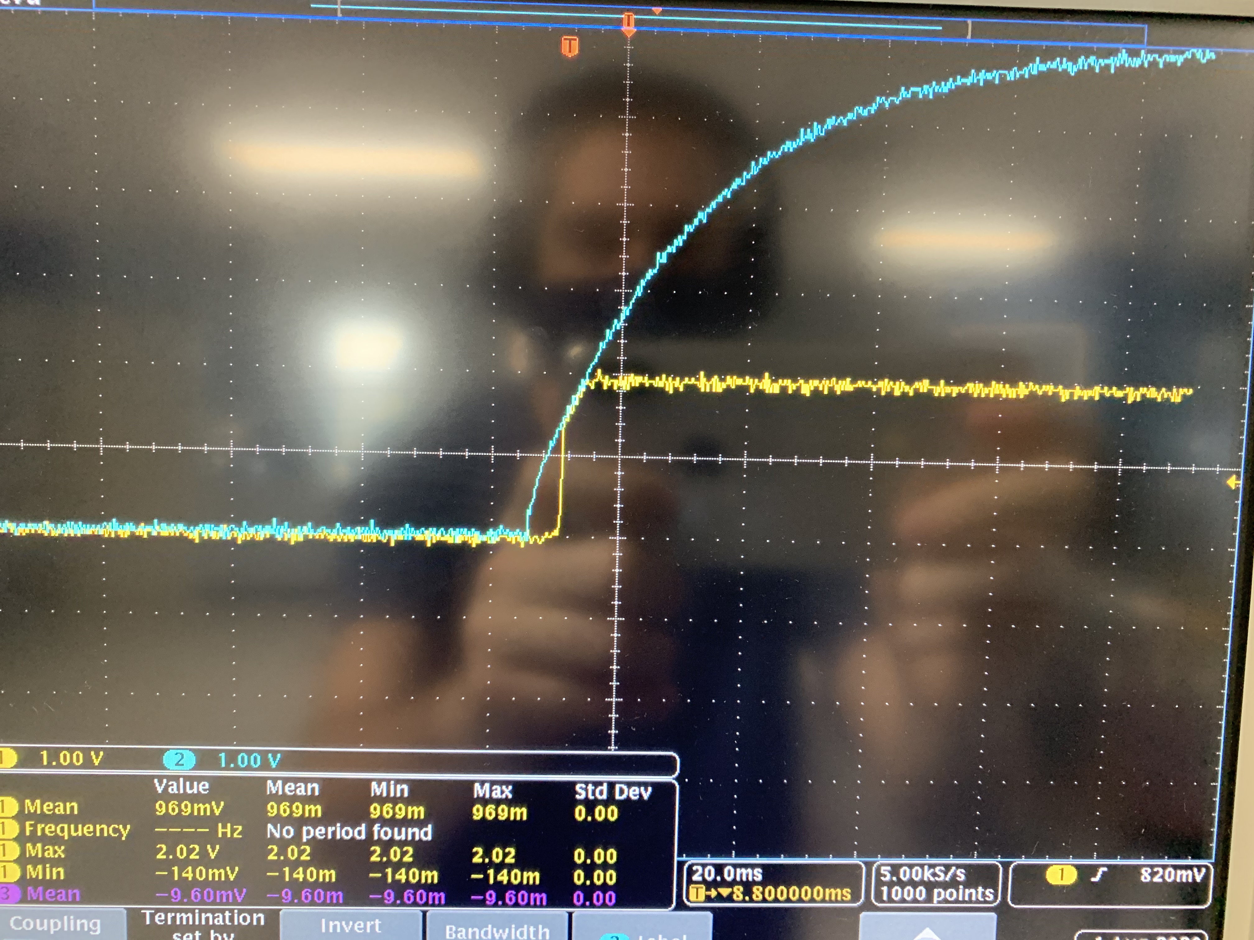
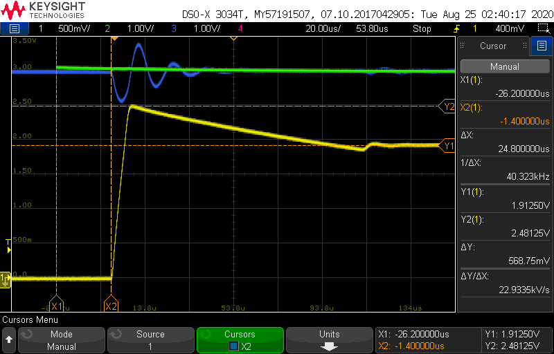
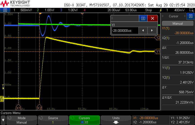
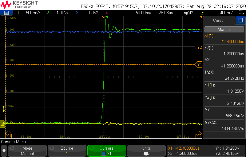
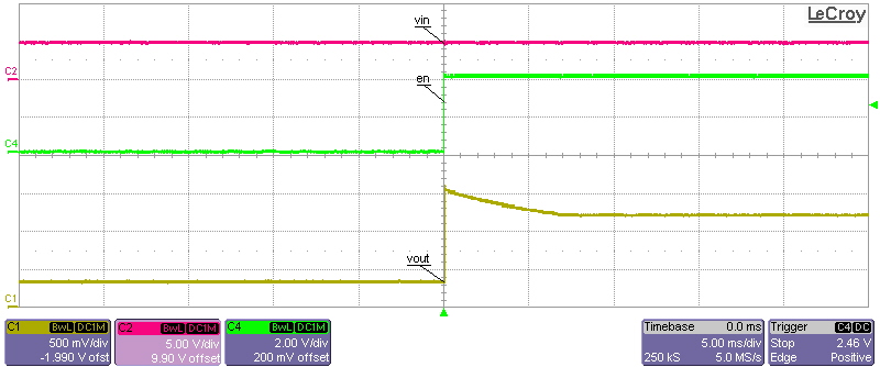
I'm experiencing the same overshoot issue when taking the TPS7A4501 out of reset.  I can't recreate it in the TINA simulator though.  What feedback was given to the original question I tagged to start this thread.

Thanks,

Nathan

  • Nathan,

    Thanks for the question.   I will post this same reply to the original question.

    It was determined that an extremely long transition time of SHDN can cause the overshoot to occur.

    The datasheet will be going through a revision in the near future, and there will be information added to identify this.

    The circuit used an RC delay to inhibit turning on the LDO with pullup on SHDN.  The turn on delay was in the order of multiple ms.

    It would be recommended to use a Schmidt trigger if the SHDN is being driven by a slow rise time signal.

    If this answers your question, please click "This Resolved My Issue"
    Regards,
    Wade

  • We have found the overshoot occurs even when we have a fast edge on SHDN# (controlled directly from an FPGA pin). We’ve also discovered the overshoot only occurs when SHDN# is driven high after power is already present on IN, which we need to do in our application. We’ve replicated this overshoot with the TPS7A4501 eval board too. Do have further guidance for a way to eliminate the overshoot?


    Thanks,

    Nathan

  • Nathan,

    Can you provide more details on the conditions used?

    Load resistance and capacitance, Vin, Vout.

    If you have schematic you can share and any scope plots.

    Thanks,

    Wade

  • Wade,

    Another engineer on my team is working this overshoot issue and had this to say in response to your last response (referenced JPGs are attached in referenced order at the end):

    While using the TPS7A4501DCQR, it was noticed that if the regulator was enabled AFTER power was applied, that overshoot would be seen on the output rail (Overshoot_No_Changes.jpg). We initially suspected inrush, and changing the output capacitance on the rail had some effect, but did not fully correct it, even after removing nearly all capacitance on the line. 

    It was also noticed that some rails on our designs, as well as on the eval board, showed a nice, gradual increase up to the final voltage (Eval_Board.jpg). We finally pinned down that it was only the rails that were being sequenced via the SHDN line that were having issues. After making that discovery, the eval board was tested by simply starting the regulator in the OFF position, then transitioning to the ON position while power was applied. Once that was done, the eval board began exhibiting the same behavior of overshooting that we were seeing on our boards.


    As far as we can tell, this issue seems to be unrelated to the amount of time that it takes for SHDN to ramp (faster or slower makes no difference). We believe that the issue is that the error amplifier is defaulting to a full on state on powerup, which is then shorting VOUT and VIN. The error amplifier then takes a longer time to compensate for the extra current, resulting in the overshoot. This means that the second portion of the rise time seen on the eval board is actually not intentional – it’s the slew rate being limited by the ramp time of VIN (VIN_vs_Vout.jpg).


    We’re currently planning on moving the control of this external to the IC to make sure that we can ramp both of them together. We’ve also tried a number of different values for the compensation capacitor with not much effect (except on the noise). Is there anything that we can do to mitigate this issue without the use of external circuitry?

    Thanks,

    Nathan

  • Nathan,

    Thank you for the plots.

    I will confer with designer, and will also schedule time in the lab to verify behavior on my lab boards.

    I noticed that you are using the commercial version of the device.   They do share the same base design, but there are processing and packaging differences that may influence device performance verses the space qualified versions.

    What eval board are you using? 

    TPS7A4501EVM-385 Evaluation Module

    Or the TPS7A4501-SP wide-VIN low-dropout (LDO) voltage regulator evaluation module

    What device (part number) is planned for use in your system?

    Regards,

    Wade

  • Wade,

    I'm the engineer who took the scope shots in the previous post + wrote the write up. The part that we are using is the TPS7A4501DCQR.

    We are using the TPS7A4501EVM-385 board. I modified it to use the DCQR package just to make sure that it uses the same package that we are using. I've also removed some of the output caps except for a 10uF ceramic to simplify things. Load resistance is 50Ohms, but I've also tested this circuit out with high loads all the way to low loads and have seen similar behavior.

    The first scope shot is actually of the TPS7A4501DCQR on our board, in circuit after being powered on. The second two are the eval board.

    If it would help, I can generate a schematic that represents what we've done to the eval board if it helps the people on your end figure out what's going on. If there's an eval board handy over there, I'd recommend powering up the board with it in the OFF position, then moving it over to the ON position. You might see some bouncing issues, but I've found that to be a decently reliable way to get the LDO to overshoot.

    Let me know what additional info you need, and I'll get it to you.

    Daniel

  • Daniel,

    Thanks for the information.  

    I will get this thread moved to the appropriate team to support.  The product selected was the space rated version of the LDO and the system routed it to the Space power team.  I will follow the thread, as it may also relate to the space rated version.

    Regards,

    Wade

  • Wade,

    Who/where should I expect follow up from? I haven't seen any activity on this or any related topics pop up in the past few days, so if this needs to be reposted in the relevant area, just let me know.

    Thanks,
    Daniel

  • Daniel,

    You should get a reply from the owning product group same as you receive this message.

    I will ping the owner to make sure they received notification properly.

    Regards,

    Wade

  • Hi Daniel, 

    Sorry for the delay. I have reviewed your previous conversation with Wade. Normally sequencing EN (or /SHDN) after Vin fully ramped up should give less overshoot. For some reason, your results showed differently. 

    One thing I have noticed is that your input signal is actually ramping up very slowly and when the VIN is connecting to /SHDN, the slow ramp allows adequate time for the error amp to transition from fully on without causing a noticeable overshoot that will normally be seen with a much faster Vin ramp without sequencing. 

    I have a question on the plot you shared that shows an overshoot when you have an external control on the /SHDN, do you have a plot that shows the Vin level when the /SHDN has been quickly toggled on? I would like to make sure Vin is already at a level higher than the set output before toggling /SHDN. 

    Regards, 
    Jason Song

  • Jason,

    Just to make sure I understand your request properly - you are asking for a scope shot that shows VIN at steady state, with SHDN toggling after, correct?

    My initial scope shot shows that scenario - VIN isn't shown there because it's steady state out of a linear supply, which wasn't very interesting.

    If that's what you're asking for, I can get those to you Monday.

    Daniel

  • Hi Daniel, 

    I found one of the startup plots we took using the TI EVM for the non-SP part, and as you can see from the thread, the startup waveform looks very clean and without obvious overshoot. Please take a scope-shot that is similar to the one in the thread in which Vin, SHDN, Vout are clearly shown in the same plot.

    Regards, 
    Jason Song

  • There is another post that also shows the startup of the TPS7A45. 

    https://e2e.ti.com/support/power-management/f/196/t/717424

  • Jason,

    I'm definitely not seeing the same delay that is showing up in the other posts. It looks like the other posts have roughly 40 - 60us of delay between SHDN toggling and VOUT being enabled. I'm not entirely sure if this is due to the package difference between the parts we are using - I've modded my EVM to use TPS7A4501DCQR, while the linked posts were using the default TPS7A4501KTTR. I've ordered some replacement parts to get the eval board back to its default state to verify.

    Thanks,
    Daniel

  • Hi Daniel, 

    In the scope-shot you just uploaded, CH1 is the output, CH2 is the SHDN, and CH3 is the input. It would be better if you could also show the delay from SHDN (low->high) to the output (low-high). 

    Looking at the other plots collected using TPS7A45 EVM, this part does seem to have a built-in soft start which would result in a controlled monotonic ramping up. In addition to evaluating using the dedicated TPS7A45 EVM, I would also suggest checking if you have the right TPS7A45 unit on the board. I would not expect the startup behaviors to be that different from the same die but different packages. 

    Please let me know once you have more data to share. 

    Thank you, 
    Jason

  • Jason,

    Yes, the channels are in the order you described. VIN is steady state when power is supplied, and is from a linear supply. I'm not quite sure what the request is for the scope shot. Do you want VIN to ramp up in the same scope shot as SHDN ramping up?

    I'd like to point out that we are seeing this on all of our sequenced LDOs currently on boards right now (designed by multiple designers as well), so this is definitely not an isolated issue.

    The DCQR footprint is somewhat compatible with the KTTR footprint, which is how I modified the board. Would it be possible for someone on your end to give that a shot as well?

    Daniel

  • Hi Daniel, 

    Yes, the channels are in the order you described. VIN is steady state when power is supplied, and is from a linear supply. I'm not quite sure what the request is for the scope shot. Do you want VIN to ramp up in the same scope shot as SHDN ramping up?

    --Yes, please have SHDN and Vout ramping up in the same plots. For the Vin, since it's steady, please just include the signal in the plot.

    The DCQR footprint is somewhat compatible with the KTTR footprint, which is how I modified the board. Would it be possible for someone on your end to give that a shot as well?

    --Let me order some EVMs and DCQ samples on our ends and if needed, we could help to evaluate the board as well. In the meantime, have you tried to check with KTT package? 

    Regards, 
    Jason Song

  • Jason,

    Please see the previously attached image - I believe that's what you're asking for. VIN has a bit of ripple once the load is applied, but you can see SHDN and VOUT clearly in those pictures. One thing I'm doing slightly differently is measuring the time between SHDN going high and when VOUT starts to rise, instead of measuring when it reaches steady state due to the overshooting issue. When comparing that time frame between the previously attached threads/plots, we're still well under the startup time shown in the other threads.

    The KTTR parts are en route, and I'll hopefully have results tomorrow or Thursday, depending on when they arrive.

    Thanks,
    Daniel

  • Hi Daniel, 

    The latest scope shot you attached did not show the low-high transition of the SHDN and when you are doing your new comparison, please having it so we could read the startup time from the scopeshot. 

    I have placed an order for the EVM and the DCR samples but for our internal samples, they only ship via ground shipping, which could take up to 5 business days. 

    Regards, 
    Jason Song

  • Jason,

    I think you're mistaken. CH2 shows SHDN transitioning from low to high. The rising edge happens very quickly, so it is difficult to see the line. The time delay that I have measured in that plot goes from the SHDN transition to when VOUT starts to rise. If you look closely, you'll see that there is no HIGH line on SHDN prior to the far left cursor.

    I can zoom in on that area if you'd like to see the rise time of SHDN instead? I just won't be able to show that and VOUT in the same plot.

    Thanks,
    Daniel

  • Hi Daniel, 

    Okay, thanks for the explanations and if so, the plot is good. Please let me know once you have some test data with the KTT parts. 

    Regards, 
    Jason

  • Jason,

    Here are the plots with the KTTR package. The delay between SHDN going high and VOUT starting to rise appears to be slightly longer with the KTTR package, but the performance is otherwise identical.

    I'm using a function generator to toggle SHDN, so the edge is nice and quick.

    Based on this, it looks like the package isn't the culprit here. 

    Thanks,
    Daniel

  • Hi Daniel, 

    In addition to the plots you shared, have you ever shared your schematic for us to review? What have you modified on the EVM? The results you shared make me think something is quite different on your boards than the default configuration of the EVM. 

    Regards, 
    Jason Song

  • The only difference between the stock EVM and our board is that R1 and R2 have been configured for 1.925V out and we are toggling SHDN with a function generator instead of the jumper to make sure that we have a good, clean transition.

  • Hi Daniel, 

    Will you provide the values of R1 and R2 on your boards? 

    Regards, 
    Jason

  • R1 = 1.69k

    R2 = 1k

    Output voltage should be a little over 1.925V, which the scope shots show we're getting (1.9125). If you're concerned about that 100mV, I can remeasure more closely to ensure better accuracy.

    Daniel

  • Hi Daniel, 

    Sorry for the delay. Have you tried to use the EVM with the default R1 and R2 and with 3.3V output? For some reason, our bench results are very different than yours. Please let us know once you have verified it with the 3.3V. 

    In the meantime, is it possible for you to take a photo of your test setup? I am trying to understand where the difference could be. 

    Regards, 
    Jason Song

  • Jason,

    Changed the output to roughly 3.3V with R1 = 1k and R2 = 1.78k. Load resistance is 50Ohms, just to get some current flowing. Function generator output is connected to pin 2 on JP1 with a 3.3V pulse every 2 seconds. Delay between SHDN toggling and the output rising is still about 27 - 28us. Still seeing the same overshoot.

    When your team is testing the eval board in the lab, how are they powering up the board/toggling the enable line? Like I said before - this is far from an isolated issue for us - we're seeing this on every design that uses this part that has external sequencing.

  • Hi Daniel, 

    I will be in the lab on 9/3 and I will check this again with our EVM and provide you all the details about my testings. 

    Regards, 
    Jason 

  • Hi Daniel, 

    I tested the TPS7A45 using the EVM using the default configuration which has FB connecting to the GND. I do observe overshot. I apologized, but the previous scope shot in the forum may have issues. 

    It seems to me that this device does not have a built-in soft-start, which could result in an overshoot. At step, are you open to another IC? 

    Regards, 
    Jason Song

  • Jason,

    Appreciate the confirmation. Do you have any recommendations for a similar IC? Maybe something functionally identical to this chip, but that does have a soft start circuit?

    Thanks,
    Daniel

  • Hi Daniel, 

    To help other customers, I am posting the scope-shot I got yesterday with TI EVM with FB connecting to the output. This is to confirm the startup did show overshoot for TPS7A45. 

    I will get back to you soon with a device that does have the built-in soft-start. 

    Regards, 
    Jason Song

  • Hi Daniel, 

    To give you the best part for your application, I can see you are doing a 6V to 3.3V conversion but what is the load current you would use the device for? Are you looking for a particular package? 

    Regards, 
    Jason

  • Jason,

    We can always update layouts to accommodate a new package, assuming it's not drastically larger.

    Otherwise, something identical in specification to this regulator would be ideal. We were using it as a general purpose LDO, so we have a use case for pretty much every scenario (high current, low current, parallel regulators, sequenced, unsequenced, noise sensitive, etc.). The closer it is to the TPS7A4501, the less analysis we'll need to update.

    Thanks,
    Daniel

  • Hi Daniel, 

    I am forwarding your request to our marketing team and I will get back to you as soon as I hear back from them. 

    Regards, 
    Jason

  • Hi Daniel, 

    We are still checking, and we will get back to you soon. 

    Regards, 
    Jason Song

  • GPN TPS7A45 TPS7A47 TLV767
    AEC Q100 NO NO NO
    Output Options Adjustable Output, Fixed Output Adjustable Output, Programmable Output Adjustable Output, Fixed Output
    Iout (Max) (A) 1.5 1 1
    Vin (Max) (V) 20 36 16
    Vin (Min) (V) 2.1 3 2.5
    Vout (Max) (V) 20 34 14.5
    Vout (Min) (V) 1.5 1.4 0.8
    Fixed Output Options (V) 1.5, 1.8, 2.5, 3.3 - 0.8, 1.8, 2.8, 3.3, 5
    Enable YES YES YES
    Power Good NO NO NO
    Output Capacitor Type Ceramic Ceramic Ceramic
    PSRR @ 100KHz (dB) 38 60 53
    Noise (uVrms) 35 4 60
    Accuracy (%) 2.5 2.5 1
    Vdo (Typ) (mV) 300 307 900
    Iq (Typ) (mA) 1 0.58 0.05
    Thermal Resistance θJA (°C/W) 28 33 60.1
    Min Package Area (mm2) 45.89 25 4
    Package Type DDPAK/TO-263, SOT-223 VQFN HVSSOP, WSON

    Daniel and Jason,

    The best options available are TLV767 and TPS7A47. The comparison is in the table and the device choice will depend on your application. Please let me know if you have any other questions.

    Thanks & Regards,

    Prakash L

  • Prakash,

    Thanks for the part numbers. We'll take a look and see what the impact is for our designs.

    We also looked at the TL1963 as a potential drop in replacement, but it appears that this exhibits a similar overshoot behavior on startup.

    Thanks again,

    Daniel

  • Hi Daniel, 

    The built-in soft-start function is a relatively new feature that has been added to the LDO design, most of the old LDOs do not have this. Please let me know if the two recommendations would meet your needs, if not, please do let us know. 

    Regards, 
    Jason Song

  • Jason,

    Understood. However, given that these parts have an Enable feature, how does TI recommend that it is used? We have a solution that essentially moves the Enable functionality external to the IC, but is there another recommendation that you have?

    Thanks,
    Daniel

  • Hi Daniel, 

    If the Vin ramp in the application is really slow, using a separate digital IO or analog output on EN to turn on the device is preferred to minimize any potential overshoot. For fast Vin ramp, you could have Vin and EN connected together. 

    More details about this recommendation can be found in chapter 2.4 of this app note. 

    Regards, 
    Jason Song

  • Jason,

    Just to make sure I'm understanding this correctly:

    TI's recommendation is to make sure that VIN ramps very quickly so that Vref does not track to VIN, which otherwise would cause the error amplifier to force the pass element to full on.

    However, our scenario has VIN already full on and stable when EN is toggled, meaning that VIN and Vref shouldn't be ramping at all, or at least, VIN's effective slew rate is "infinite" in this scenario.

    Wouldn't that mean that the issue more likely occurs when the startup time is faster than the loop compensation bandwidth of the device?

    Thanks,
    Daniel

  • Hi Daniel, 

    TI's recommendation is to make sure that VIN ramps very quickly so that Vref does not track to VIN, which otherwise would cause the error amplifier to force the pass element to full on.

    --Yes, this statement is true for most of the LDO design. For the other two recommended devices, this will apply.

    However, our scenario has VIN already full on and stable when EN is toggled, meaning that VIN and Vref shouldn't be ramping at all, or at least, VIN's effective slew rate is "infinite" in this scenario.Wouldn't that mean that the issue more likely occurs when the startup time is faster than the loop compensation bandwidth of the device?

    --For some reason, TPS7A45 does not follow that statement and this is part that confused me at the beginning. 


    Regards, 
    Jason Song

  • Jason,

    Assuming that I'm on the right track for the TPS7A45XX series, is there a way that I could extend the loop compensation bandwidth via the VOUT or ADJ pins? Bit of a long shot, but just want to make sure I exhaust my options.

    Thanks,
    Daniel

  • Hi Daniel, 

    If overshot is critical for your application and the LDO has no built-in soft-start or in-rush control, it would be difficult to completely eliminate the overshot. You could try to increase the output capsize, or consider adding a feedforward cap between output to ADJ, or try different Vin ramps with Vin connecting to EN to see if it helps. They may all help to an extent, but it requires a lot of testings, and the device may also have part-to-part variation. 

    How the overshot will impact your application? 

    Regards, 
    Jason Song

  • Jason,

    During my initial tests I made a circuit that pulled out the enable feature via some external FETs.

    Changing the ramp rate of the control FET appeared to be sufficient to eliminate the overshoot. What I found was that rather than controlling the loop compensation bandwidth on the output, it was a little more straightforward to simply let VIN short to VOUT, but make it so that the ramp rate of VIN was inside the loop compensation bandwidth of the LDO.

    The end result is that you see the input ramp on VOUT, but you eliminate the overshoot. It also minimizes the potential for inrush current ringing/overshoot from using a similar setup on the output side.

    We've experimented a decent amount with the feed forward cap for the purposes of reducing noise, but not for affecting the overshoot. I'll take a look at that in the future.

    Thanks,
    Daniel

  • Hi Daniel, 

    Yes, if you have a very slow Vin ramp and are not planning to use SHDN to turn on the device, you could eliminate the overshot. Is this what you plan to do in the application? 

    Regards, 
    Jason