This thread has been locked.

If you have a related question, please click the "Ask a related question" button in the top right corner. The newly created question will be automatically linked to this question.

UC2854B: PF was low

Part Number: UC2854B

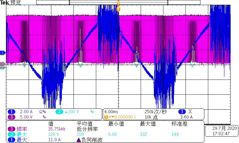
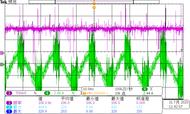
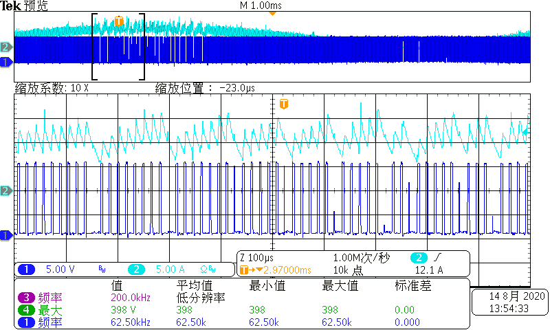
I cannot get the ideal PF, I designed a 3kilowat PFC, but when I added load to 1KW, the PF was 0.94.

  • Hello ,
    The pfc is designed for best power factor at low line and full power.
    As the line voltage increases and the power decreases the power factor will decrease.

    This is because the capacitor on the DC side of the bridge rectifier tends to charge up with a residual DC voltage below the instantaneous value of the AC line.
    This will prevent the AC line from supplying current at this interval .The result is a degradation in power factor.

    If your design is for a 3kW load and you get a pf of 0.94 at 1kW then it will be difficult to improve this value.
    Have you tried decreasing the value of the capacitor?

    Regards

    John

  • Dear John,

    Thank you so much for your reply. I think there must be some elements that i missed. This is the photo when the pf was 0.94. Do you have more ideas? Thank you

  • Hi,
    What are the test conditions for this waveform?
    Do you get a good waveform at any load or input voltage?
    I can see that the pwm is very unstable at the peaks and it may be the current loop is not responding properly.
    What is waveform channel 2 ?

    Can you provide the schematic for review ?

    Regards

    John

  • This was the waveform when PF was low. Ch3 was waveform of CA out. CH4 was input voltage

  • This was the waveform  when PF was 0.99. CH3 was CA output. CH4 was input current. At input 176Vac , PF was OK(When the load was 400W, the PF would be 0.99).But at 220Vac, when the load was 2KW, PF was 0.98.,

  • 2854.pdf

    This is the SCH.

  • Hello ,
    It looks like the pfc is going into peak current limit and shutting down the pwm.
    In your schematic the multiplier output is set for a 20A peak input current and the peak current limit is set for a 75A peak fault current.
    These values all look ok and so I dont know why the current waveform looks so bad with only a 1kW load.

    Can you please double check these values:

    .02 Ohm sense resistor

    10k from VREF to PKLMT

    2k from PKLMT to negative side of .02 Ohms 

    2k from MULT to negative side of .02 Ohms.

    Everything else in the schematic looks ok but it seems that as you increase the load the system shuts down.

    Perhaps you can use a scope probe on GTDRV and monitor what happens during this strange event.

    Regards

    John

  • Thank you, John.

    I did check up the pins yesterday. Down Pic 1 was the PKlMT  at 220Vac which was CH3, CH4 was input current. Pic2 was PKLMT at 176Vac. Really cannot see the big difference

  • Can you look at the gate drive signal and see how it is behaving during these spikes ?

    One of your waveforms above shows CAOUT going to zero during this spike sequence.
    You need to figure out why this is happening because with CAOUT equal to zero the PWM is maximum.
    CAOUT goes from being ok to really wrong. 

    Is VCC and REF properly decoupled ?
    You need an X7R ceramic capacitor in 1206 or 0805 package placed directly on the VCC and REF to GND of the controller

    Regards

    John

  • Hi John

    Sorry replied so late.

    At those abnormal  moment, there was no drive signal. It would turn off for one switch circle for the moment when the input current dropped. It would last for 5 or 6 times before it returned notmal again.

    Here is the pic. CH1 was Vgs of MOS, CH2 was L current. Is there a possibility that it was caused by minimum ducy cycle?

  • Hi Raven,

    The gate drive is turning off because the system is unstable. The large peak current are due to the pwm being too high and when the system realises this 
    it repsonds by turning off the pwm.
    The question is why is this instability happening. Have you looked at 
    (1) The error amplifier compensation loop
    (2) Noise pickup around the current sense amplifier
    (3) Check the waveform on VCC and VREF.
    Is there any system noise here during load due to pcb layout.
    The issue only seems to occur at higher load so this makes me suspect that there is a layout problem.

    Regards

    John