A related question is a question created from another question. When the related question is created, it will be automatically linked to the original question.
If you have a related question, please click the "Ask a related question" button in the top right corner. The newly created question will be automatically linked to this question.
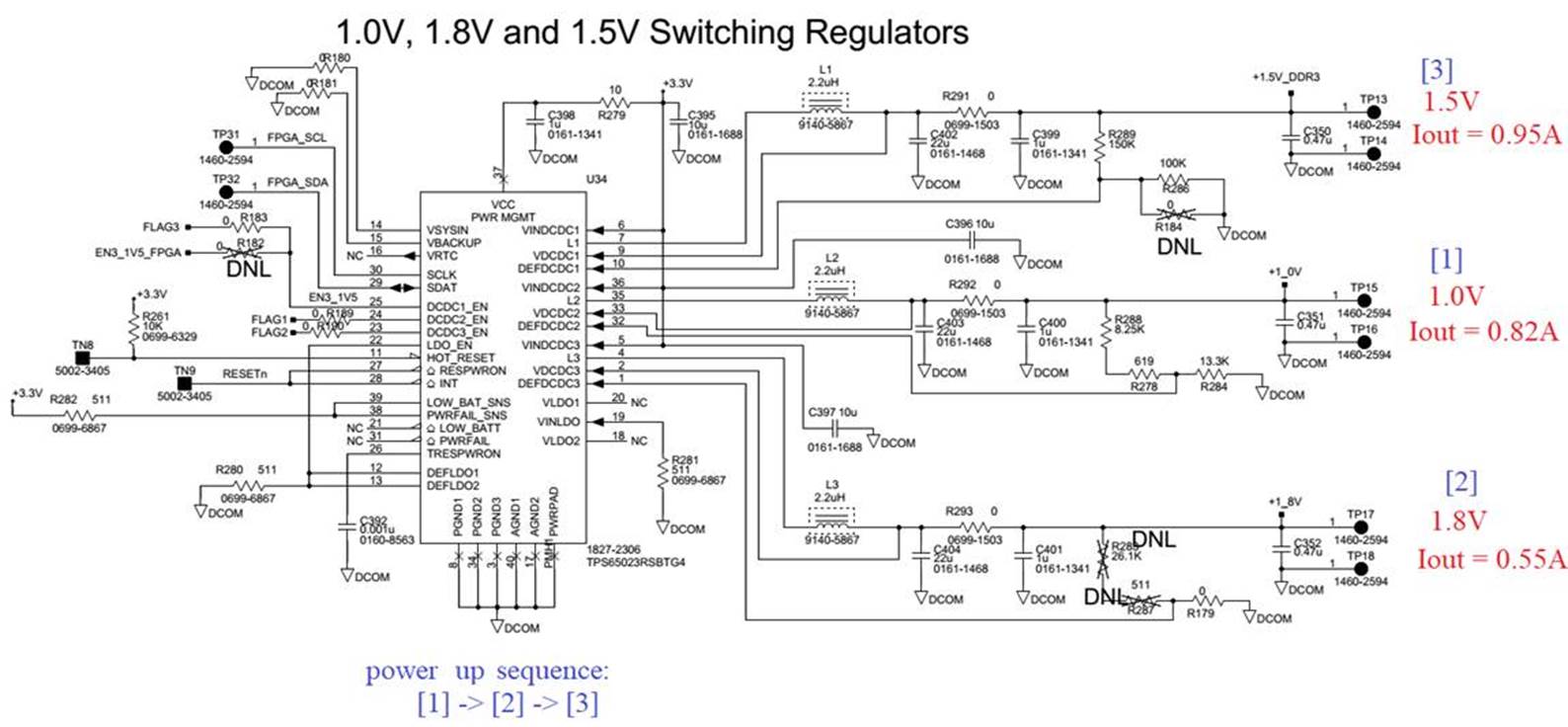
TPS65023: Request help to review schematic design using TPS65023RSBTG4
In the text editor, you need to click the paperclip symbol (says "Insert File" if you hover over) to attach a PDF or other file type or the Image+ symbol (says "Insert/Edit Media" if you hover over) to insert an image (.PNG, .JPEG, .GIF) in the body of your message.
Both symbols are highlighted in the below image, which was inserted using the Image+ symbol to "Insert/Edit Media" and added a .PNG screen shot saved on my PC.
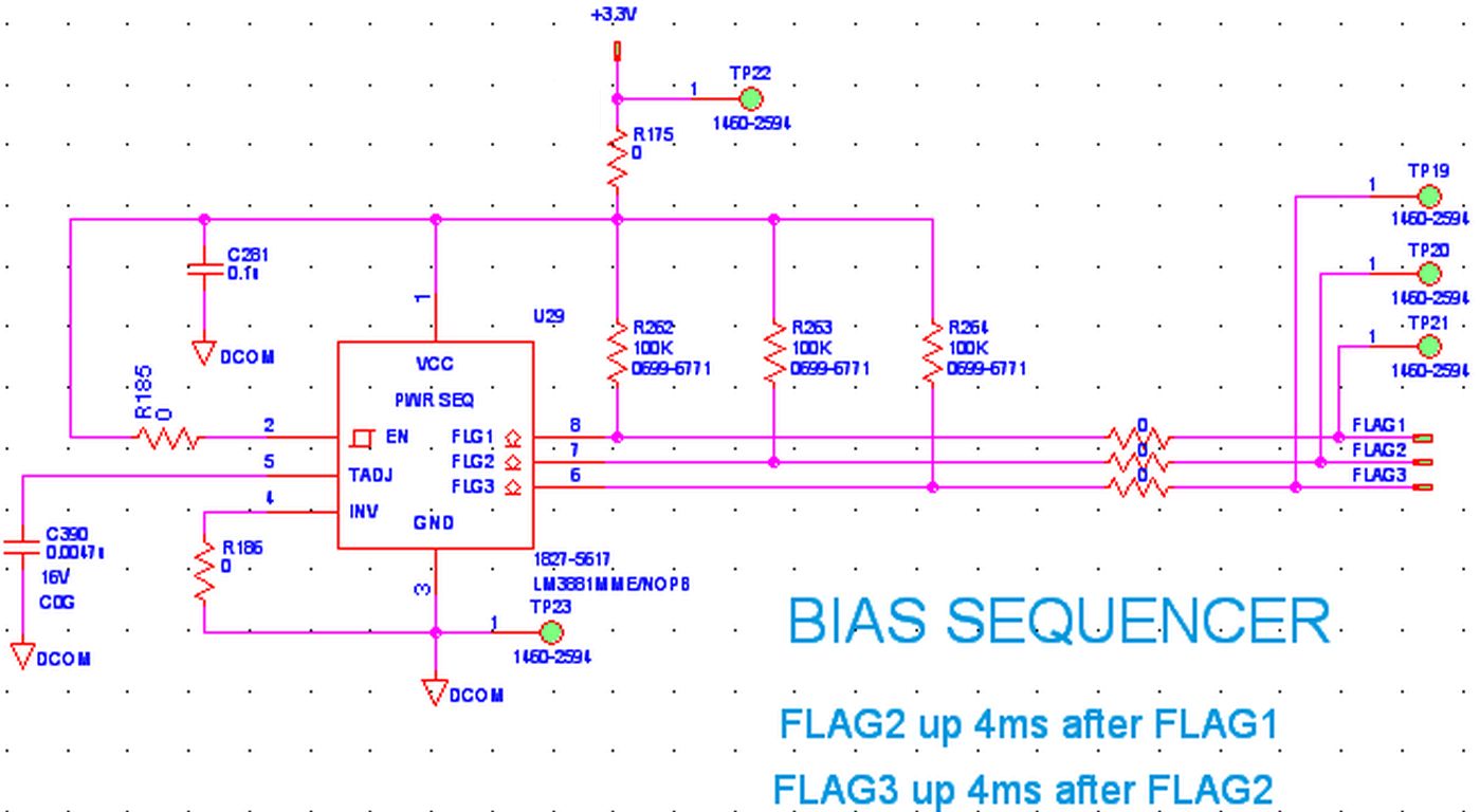
Result: when EN pin of LM3881 is >1.22V (t0), the sequencer will start operation. Since INV = GND (Low), FLAGx outputs are active-high which is correct for controlling the TPS65023 PMIC.
1.0V (DCDC2) will be enabled by FLAG1 at time t0 + TD1
1.8V (DCDC3) will be enabled by FLAG2 at time t0 + TD1 + TD2
1.5V (DCDC1) will be enabled by FLAG3 at time t0 + TD1 + TD2 + TD3
T_enable_delay = 1.22V * CEN / 7uA = 0 because there is no capacitor at the EN pin to create an RC delay during startup. When "+3.3V" net > 1.2V, sequencer will start.
The image is hard to read, but it looks like the capacitor at TADJ pin, C390, has a value of 0.0047uF
TADJ,period = 120us/nF*0.0047uF = 0.564ms
TD1 = 9*0.564ms = 5.076ms Min, 10*0.564ms = 5.64ms Max
TD2,TD3 = 8*0.564ms = 4.512ms typical
These are the sequence order and timing parameters for the LM3881 as it has been implemented in your system.
Since I do not know the FPGA that is being powered the TPS65023 device, you will need to determine if the sequence timing and order will meet the sequencing requirements of the FPGA.