This thread has been locked.

If you have a related question, please click the "Ask a related question" button in the top right corner. The newly created question will be automatically linked to this question.

UCC28950: SLUA560C mosfets at the secondary side

Part Number: UCC28950
Other Parts Discussed in Thread: TINA-TI, PMP8787

Hi, 

Hope you are doing good.

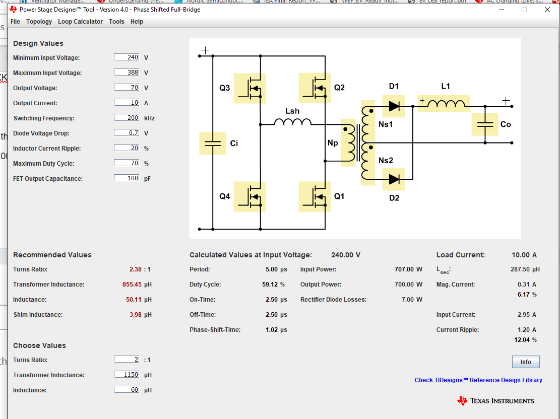
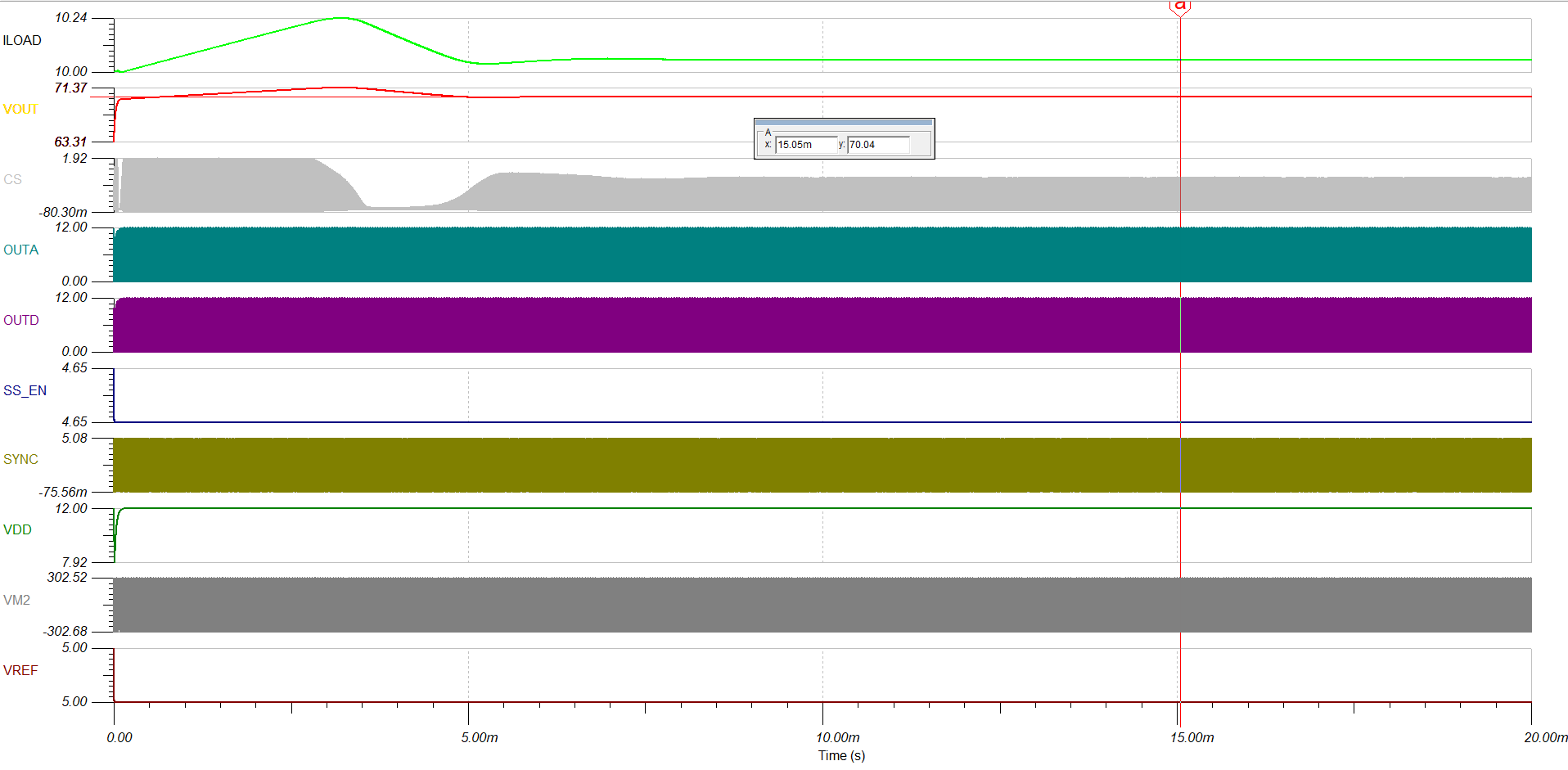
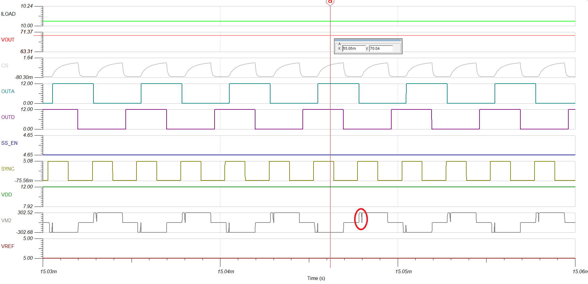
We are following SLUA560C reference design to design a 70V DC, 10A, 700 W smps with input  of 170V to 275 V AC.

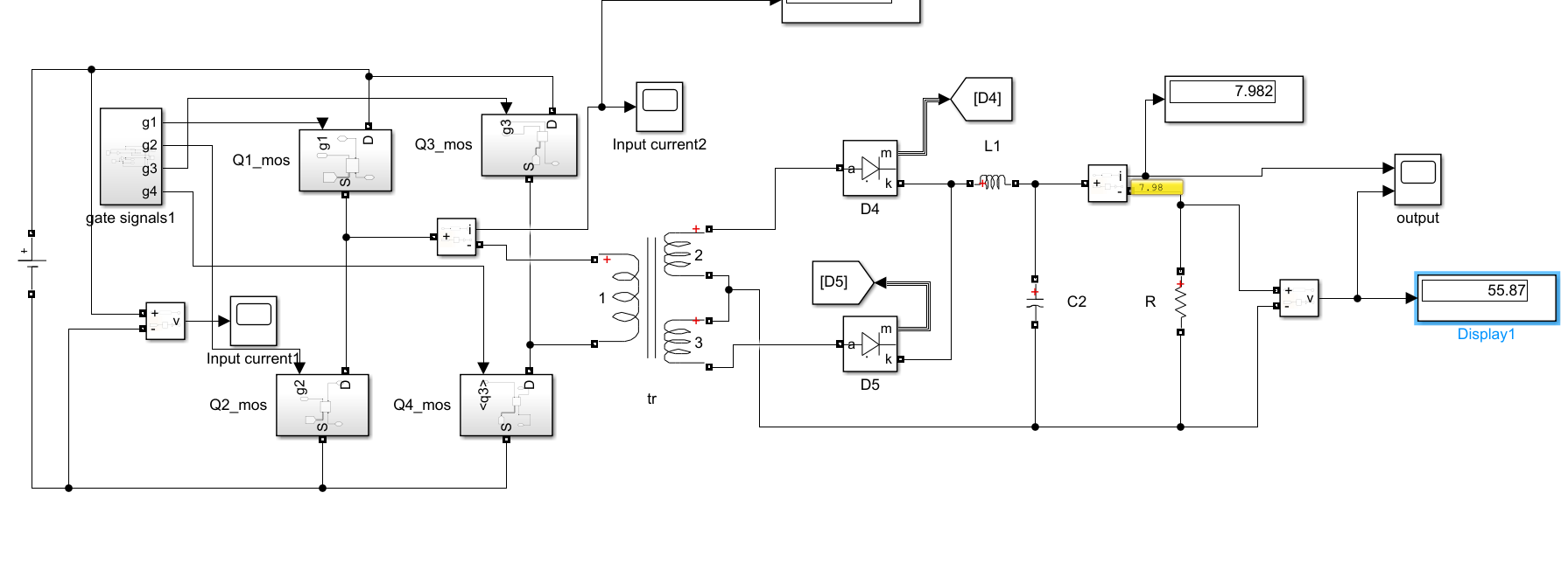
at the same time we are using power stage designer tool for phase shift full bridge design. 

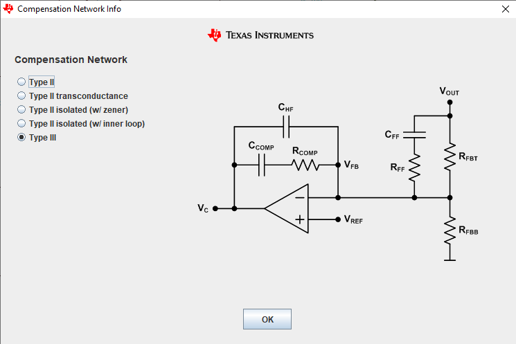
In the power stage design tool, on the primary side, there are 2 diodes where as on the SLUA560C there are two mosets.

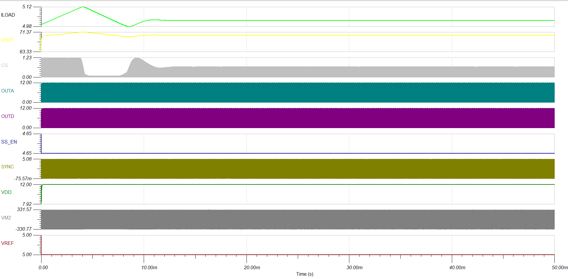
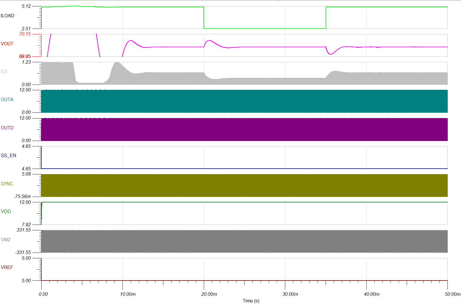
We are trying to design the SMPS with 94% efficiency. 

when it comes to the selection of components and the Pbudget calculations, 

We are running out of the calculated budget to accommodate the input capacitor losses and the the mosfet power losses at the secondary side. Please find the attached excel sheet SLUC222D (version 1).xls

We are using the following parts 

Qa,Qb, Qc, Qd mosfets: IPA60R145CFD7XKSA1 (part number)

Ls(shrimp inductor) : B82477P4392M 

Cout : LKMD1151K820MF

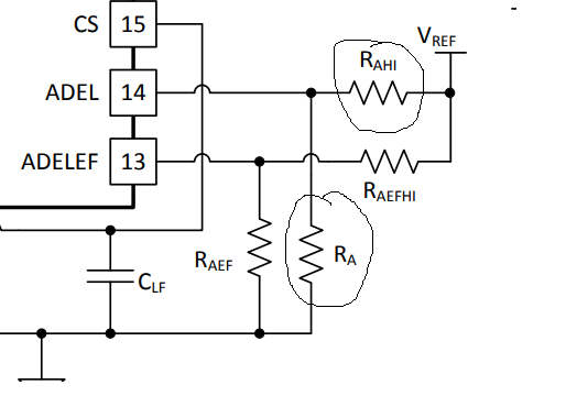
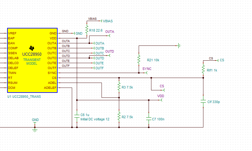
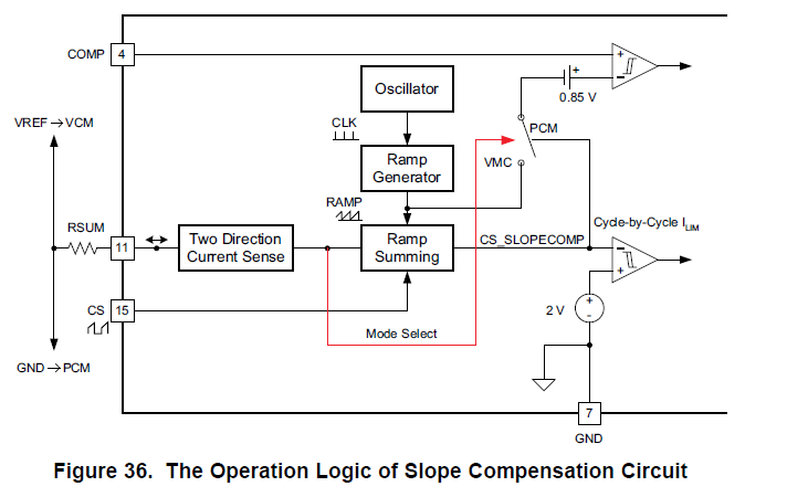
What is the purpose of having 2 mosfets at the secondary side instead of diodes?

on page 11 of UCC28950 600-W, Phase-Shifted, Full-Bridge Application Report, the calculated voltage across secondary fets are Vin(max)/a, we have 388 Vin max and the turns ratio is 2. the voltage across fets on secondary should be 194V. but on the calculation tool, it reads 388V. for the selection of mosfet at secondary, which value should we go with? could you please suggest on this?

https://www.ti.com/lit/an/slua560c/slua560c.pdf?ts=1596045656345&ref_url=https%253A%252F%252Fwww.google.com%252F

could you suggest parts for 70V DC, 10A, 700 W design so that twe can have efficiency of 94 % or above?

Thank-you

Warm Regards

Harini Krishna

  • Hello Harini

    There is a typo error in the App note the voltage stress is Vin/2*a1 so 388 is the correct answer. The reason is that the turns ratio is normally calculated as Np/Ns where Ns is the turns on one half of the centre tapped secondary. Since there are two such windings, on on each side of the centre tap the total number of turns on the secondary is 2*Ns and the total voltage across the entire secondary is twice that measured from the Centre tap to one end of the winding.

    Whether to use SRs (MOSFETs) or Diodes is a bit more difficult to decide. The absolute value of the voltage drop across the secondary rectifiers is probably going to be lower if you use SRs - certainly this will be the case for low voltage outputs. As the output voltage increases the forward voltage drop across a diode becomes a lower proportion of the total and so it has a lesser effect on the efficiency. Eg, 0.6V on a 12V output is 5%, 0.6V on 70V is 0.85%. I'd suggest you do the design both ways and calculate the estimated losses for each option. You will probably find that diode rectification allows you to meet your efficiency target.

    Regards

    Colin

  • Hi Colin,

    thank-you for the reply.

    Can you suggest the diode for our application?

    can you guide us in deciding the diode specifications?

    Thank-you

    Warm Regards

    Harini Krishna

  • Hi Colin,

    Hope you are doing good.

    I have a few doubts regarding power stage designer tool. 

    what does the following terms refer to?

    transformer inductance 

    Inductance (  is it value of L1)

    Lsec

    Mag. current 

    input current 

    The terms are a bit confusing.

    Can you please help us with this?

    Thank-you

    Warm regards

    Harini Krishna

  • Hi Colin,

    Regarding the power stage designer tool, 

    We figured out the terms by hovering the mouse over the value. 

    We tried to build a matlab model for our requirements, 

    Input : 240V  to 388V DC
    Output :  70V, 10A. 

    on a n ideal scenario, we are reading 9.975A and 69.83V at the output. ( all the transformer leakage inductance 0)

    but we are measuring very high input current at the primary side( we are measuring 143A with an ideal transformer)

    Thank-you

    Warm Regards

    Harini Krishna

  • Hello Harini

    I'm afraid I won't be able to help you on this - I have no experience of Matlab and don't have it installed on my laptop. I can only suggest that you look at the details of the start-up process you are modelling. I'm sorry to be so vague about this. I don't know of any of my colleagues who have experience of Matlab either. 143A is certainly too much. Have you modelled the switching stage correctly ?

    Regards

    Colin

  • Hi Colin, 

    Thank-you for the reply

    We are building a matlab model using the above referred documents and the parameters are as follows

     Vin= 325V DC

    Vout (required) =70V DC

    Fs= 200kHz

    Turns ratio: 2.38

    Vf= 1V

    L1: = 84.8uH

    T/F magnetizing inductance : 1123uH

    Cout = 1.6mF

    Leakage inductance are neglected.

    We followed the handbook formulas to calculate the duty cycle and the phase shift  at 325V input 

    and the calculated values are D= 0.5199(51.99%)

    t1= 1.29 us

    t3= 1.21 us 

    and got the following results on the simulation

    gate pulses given to the switches:

    the measured current at the primary side

    transformer voltages ( the first graph refers to the primary voltage, 2nd and 3rd graph refers to the center tap secondary voltages)

    Output voltage

    What may be causing the input current to go so high?

    What might be a reason for a wrong output observation?

    Can you please help us with this?

    Thank-you

    Warm Regards

    Harini Krishna

  • Hi Colin, 

    Thank-you for the reply

    • we are referring the SLUA560C application report to model out 700W, 70V, 10A  phase shifted full bridge application along with the power topology handbook

    https://www.ti.com/seclit/ug/slyu036/slyu036.pdf?ts=1597916618474&ref_url=https%253A%252F%252Flogin.ti.com%252F and the excel sheet calculator by TI. 

    1738.SLUC222D (version 1).xls

    we noticed that the calculated turns ratio at the power stage designer and the calculation sheet are not matching

    at the same time the calculated shim inductance on the design tool shows a value of 3.98uH where as the calculated tool shows a value is a negative one.

    In the power stage designer there are terms as transformer inductance, inductance and Lsec.

    Does transformer inductance refer to the magnetizing inductance? and inductance refer to the inductor L1 value in the diagram and what does Lsec refer to?

    should we consider the Shim inductor in the design?

    Thank-you 

    Warm Regards

    Harini Krishna

  • Hi Colin,

    While calculating the power losses for the transformer from the

     https://www.ti.com/lit/an/slua560c/slua560c.pdf?ts=1596045656345&ref_url=https%253A%252F%252Fwww.google.com%252F application note , page no. 6

    Here the values are 

    Iprms = 3.1A , DCRp= 0.215 ohm

    and Isrms = 36A. DCRs= 0.58 ohm

    When we calculated the value for the same  is 3010.852W not 7W.

    did we miss something in the calculations?

    Thank-you

    Warm Regards

    Harini krishna

  • Hello Harini

    I'm afraid there is a typo in the app note - the DCRs should be 0.58mOhm. If you use that value you get 7.14W dissipation. Do note that the comment about the calculation being an estimate is correct. It does not take account of AC effects in the windings such as skin and proximity effects.

    The Excel and Power Stage Designer calculations were generated by different people at different times - I'm not surprised that there are differences. In any case - some of the difference is accounted for the output voltage range on the Excel calculator is wider than that in the PSD calculator. The Dmax is also different. I'd suggest you set the min, max, and nom output voltage values in the Excel file to the nominal value used in PSD

    Your other questions

    Q/ Does transformer inductance refer to the magnetizing inductance? and inductance refer to the inductor L1 value in the diagram and what does Lsec refer to?

    A/ Transformer inductance is the Magnetizing inductance. Inductance is the output inductor value (L1). Lsec is the magnetizing inductance reflected through the turns ratio and measured on the secondary side of the transformer. LSEC

    Q/ should we consider the Shim inductor in the design?

    A/ The shim inductor adds to the leakage inductance and increases the energy available to drive the ZV transition. You may be able to design the transformer with enough leakage inductance to avoid the need for a separate shim inductor. I'd advise you to include the shim inductor and clamp diodes in your prototypes - you can always remove them later.

    The Matlab results - I'm not sure how to read this but it looks like the two secondaries are running in the same phase - they should be 180 degrees apart. Can you look at the phasing of the secondary.

    The primary current looks VERY high - possibly a consequence of the transformer phasing.

    I think I've covered all your questions but please let me know if I have missed something.

    Regards

    Colin

  • Hi Colin,

    Thank-you for the reply.

    Is this the correct way to calculate duty cycle and phase shift time for any input voltage using the above formulaes?

    Thank-you

    Warm Regards

    Harini Krishna

  • Hi Colin,

    • Regarding the high input current, while modeling the transformer parameters, 

    before we had Rm value to be very less (~ 3ohms) when we changed it to 200k ohm, we are reading the current to be 6.21A

    ( graph attached below : x- axis : time in sec, Y-axis - Current in A), i apologize for not mentioning the axis units in the previous post graphs.

    The value of Rm was a trial and error and we noticed that with Rm = 20k and Rm=200k ohm we have the same primary current measured. whereas the calculated primary current is 4.97A

    • We calculated the duty cycle and the phase shift from the following formulae
    • Vout = 70V
    • Vf= 1V
    • VNp= 325.84V
    • Np/ns=2.38
    • Fswitch = 200k Hz

    The calculated D= 51.85% and phase shift time was 1.20e-6 sec, however when the same were used into the simulation environment, we observed that the output voltage 64.19V

    With same D = 51.85% and phase shift time 1.32e-6 sec, we were able to read output as 70.66 V.  are we missing any critical parameter here which is causing a difference between the calculated phase shift and the phase shift at which we are reading the required output?

    Can you help us with this?

    Thank-you

    Warm Regards

    Harini Krishna

  • Hi Colin,

    the diode losses specified in the power stage designer tool,

    just to confirm, are the mentioned power loss the total power loss at the rectifier or just single diode?

    Thank-you

    Warm regards

    Harini krishna

  • Hello Harini

    Input current problem solved ? - Rm provided a low impedance path for the input current. I guess Rm is not simply the winding resistance but is intended to model something else - Core loss ?

    The formula for duty cycle is correct although the diode Vf  may not have much affect on the results at 70V out.

    Ignoring the dead times, the duty cycle of each of the switches in the PSFB is 50% in the steady state. The phase shift time can be easily calculated from the duty cycle - T = D*(1/(2*fswitch)  that should agree with the formula you provided above.

    There is a phenomenon in the PSFB called 'Duty Cycle Loss'. This is caused by the time it takes to reverse the current in the transformer primary at the start of a switching cycle - the time between the red lines in the image below - (slightly modified version of Fig 46) . A rough approximation of this time is Tdcl = Lleak*2*Ipri_pk/Vin. I suspect that this is why your Vout is lower in the simulation environment than in MatLab.

    The power loss in the rectifiers should be the total for both rectifiers. You can check this by measuring the Average current in the rectifiers and multiplying it by the Vf of the diodes. The average diode current this will be 50% of the average current in the output inductor.

    Regards

    Colin

  • Hi Colin,

    Thank-you for the reply.

    We are using diodes instead of mosfets in the secondary side.

    There are pins related to the delay between primary and secondary side switching.  ( DELEF, ADELEF, OUTE, OUTF). 

    how are these pins supposed to connected if we are not using any switches on the secondary side?

    How will it effect the device operation if this functionality is not used?

    Can you please help us with this?

    Thank-you 

    Warm Regards

    Harini Krishna

  • Hello Harini

    This is the way to use these pins if you are going to use diode rectification.

    The OUTE and OUTF pins should be left open circuit if they are not being used.

    The ADELEF pin should be connected to GND.

    The DELEF pin should be connected to GND through a resistor in the range 13kOhm to 90 kOhm.

    In addition to the above an option is to connect the DCM pin to VREF to suppress the switching signals at OUTE and OUTF pins. This will give a marginal reduction in the system noise without otherwise affecting device behaviour.

    Regards
    Colin

  • Hi Colin,

    thank-you for the reply.

    We are trying to simulate the psfb using UCC28950  on TINA TI. 

    converter parameters:

    input: 388V DC

    expected output :  70V, 10A.

    we followed the excel sheet calculator and the application note to calculate the component values.

    We replaced the mosfets on the secondary side to diodes. 

    We observed that the output current is in mA and the load voltage is just going on increasing . please find the graph attached  below

    can you please help us with this?

    i am attaching the Tina simulation file below.

    700W_rev1.2.TSC

    Thank-you

    Warm Regards

    Harini Krishna

  • Hi Colin,

    there was a wrong load value which was making the load current go very low. (instead of 7ohm it was 1kohm)

    but we observed the output voltage is going down,.

    can you help us with this?

    Thank-you

    Warm regards

    harini krishna

  • Hi Colin,

    We made few changes on the design,

    Rt = 28.75 kohm for 200khz switching frequency setting
    Css= 82nF for setting soft start time to 10ms ( removed  resistor between ss/en pin to ground )
    Rab=Rcd = 13kohm to set delay between ( OutA and OutB), (Out C and Out D)
    Rsum= 10kohm , for voltage control mode connect the pin to Vref through Rsum resistor.

    and observed that the output voltage is dropping down.

    Can you help us with this?

    Thank-you

    Warm Regards

    Harini Krishna

  • Hello Harini

    This is what I would advise

    Double check that the simulation is using the initial conditions -

    Run the sim to at least 5ms to allow it to stabilise around the normal operating condition.

    Observe the CS pin - just to make sure that the scaling is correct and that the CS pin is not reaching 2V

    The DC blocking capacitor may need some time to stabilise at its normal condition - put a voltage probe across it.

    Put a voltage probe from drain of QB to drain of QD to monitor the voltage across the transformer - includes V across the blocking capacitor

    Please let me know how you get on

    Regards

    Colin

  • Hi Colin,

    Hope you are doing good.

    Thank-you for the suggestions.

    We followed your suggestions from the previous post and observed that the output voltage is swinging between 69.33 to 71.11V.

    (VM1 is the voltage across the drain of QB to drain of QD) 

    Warm Regards

    Harini Krishna

  • Hello Harini

    There's some kind of instability in the system. During the time when Vout is rising the CS signal is at 1.93V. The 2V Cycle-by-Cycle comparator operates on the CS signal plus the slope compensation ramp so at this time the CbC comparator is operating and the system is in current limit.

    Can you reduce the load current by a factor of two and post the results please?

    Regards

    Colin

  • Hi Colin,

    Thank-you for the reply.

    We got the calculated value of transformer magnetizing inductance to be lm= 1.17mH. and we changed the lm to 1.2mH. and we observed the following results.

    With the same as you suggested we run the simulations and reduced the load current with a factor of 2  and observed the following

    We want to use voltage control method for our design.

    our input voltage range is : 240V to 388V DC

     output : 70V, 10A, 700 W

    switching frequency 200kHz

    Can you please verify the design of tina TI simulation?

    0334.700W_rev1.2.TSC

    Thank-you 

    Warm Regards

    Harini Krishna

  • Hi Colin,

    Can you please verify the design and make us understand where are we going wrong to achieve the required output?

    Thank-you

    Warm Regards

    Harini Krishna

  • Hi Colin,

    hope you doing good.

    can you please help us resolve the issue?

    Thank-you

    Warm Regards

    Harini Krishna

  • Hi Harini

    My apologies for the delay in responding - I'm running the sim now and will give you an update shortly.

    Regards
    Colin

  • Hello Harini

    I think the problem is that the system takes a little time to settle down at its operating point. Possibly due to a loop instability or possibly due to the initial Vout overshoot at the end of the Soft start interval. You can see here that the output starts coming back up at about 8ms. The other interesting thing is that COMP (VP_35) has come out of saturation at about 4.6V (you can't see it here unfortunately) and has started to oscillate with a period of about 6ms. The oscillation is sinusoidal and it looks like its amplitude is reducing a bit although it's very, very underdamped. I think there is very little if any phase margin here and the cross over frequency is probably at about 1/6ms or 166Hz.

    The controller is NOT entering a current limit - among other things VP_29 in the plot below is the voltage on the SS/EN pin.

    I'd suggest some things -

    1 let the sim run out to 50ms or so to see if the oscillation dies out - Tina-TI allows you to postpone taking data until some specified 'Start Display' time. You should also deltet the Vin. OUTB, OUTC, probes to reduce the data file size.

    2 Review the loop stability calculations.

    3/ Double check the polarity of the Initial Conditions on C4 and C3 - you might get better results - or at least results more quickly by setting the IC on these parts to 0V

    Regards
    Colin

  • Hi Colin,

    Thank-you for the suggestions.

    for the loop compensation and other calculations related to ucc28950 we are using the excel sheet calculator. 

    to run the simulations for 50ms, it is taking more than 6 hours.

    do you have any suggestion for making the run simulation fast? it is difficult to make changes and run it each time for 6 hours.

    We made the IC values of C4 and C3 to be 0 and found run the simulation till 60ms and observed vout to be 

    running the simulations for 50ms is very time consuming. if you would suggest something on this it would be very helpful.

    i see on the 12V, 600W design that the controller is configured as slave by adding a 875kohm resistor from ss pin to ground. since,  the application only has one device, is it not that the device(UCC28950) should be configured as master?

    if only one device is used will configuring it as master or slave make a difference?


    Thank-you

    Warm Regards.

    Harini Krishna

  • Hello Harini

    The Excel calculator assumes that you are using Current Mode control. You are using Voltage mode control and the loop compensation for VMC is very different to that for CMC. The details are in the document at http://www.ti.com/lit/slup340


    The practical difference is that you will need to use a Type 3 compensator for VMC instead of the Type 2 that suffices for CMC.


    I used the TI power stage designer to modify the loop compensation network for your application. I then simplified the power stage a bit by replacing the MOSFETs with voltage controlled switches which I control using the OUTx signals directly from the controller. This eliminated all of the earlier MOSFET drive circuitry.

    The result is a stable loop which simulates faster than the original circuit.


    Power Stage Designer can be downloaded at https://www.ti.com/tool/POWERSTAGE-DESIGNER  

    Here are screenshots of the loop compensation network and components I used in the sim.

    This is the Type 3 compensator. The difference between it and a Type 2 compensator is the two added components, RFF and CFF.

    After I made these changes I ran the sim out t0 50ms - unfortunately I didn't record how long it took but it was significantly less than 6 hours.

    /cfs-file/__key/communityserver-discussions-components-files/196/0334.700W_5F00_rev1.2_5F00_mod_5F00_faster.TSC

    Note, I changed the output potential divider to 10k/370R because Power Stage Designer gave me a 10k upper divider resistor as its starting point. You could change it to 45090R in PSD and let it recalculate the values in the compensation loop

    In the end:  You can see that you get an initial overshoot to about 71V and then the systme settles down to 70V with a well controlled recovery.

    You might like to check the loop stability by changing the load suddenly from 100% to 50% at about 20ms and back to 10)% at 30ms.

    Let me know how you get on.

    Regards

    Colin

  • Hi Colin,

    Thank-you for the reply. 

    We are running the simulations and would let you know the results. 

    as you said that you have replaced the mosfets with a voltage controlled switches, is it to reduce the simulation time?

    for the compensation loop calculation, in output potential divider to 10k/370R the power designer shows 10k/1620 ohm. is there any  specific reason for choosing 10k/370R?

    to push the model into prototype stage can we run the simulations having the mosfets and the driver circuit in the model?

    Thank-you

    Warm Regards

    Harini Krishna

  • Hello Harini

    You are correct, I used voltage controlled switches to speed up the simulation time. The control loop dynamics are not affected by the way in which the switches are implemented.

    10k/370 gives you a 70V setpoint - assuming a 2.5V reference. 10k/1620 gives you a 18V setpoint. I don't know why PSD uses this as a default value but I suppose they had to use something. There are some interactions between the value of the top sensing resistor (10k) and the mid-frequency gain and the zeros of the control loop and unfortunately I didn't have time to select a different output potential divider - but it would be relatively easy to use something like 2.37k Rfbb and 64k Rfbt and then use PSD to calculate the other compensation components for you.

    Once you have the simplified model up and running you can of course put the 'real' MOSFETs and their driver circuits back into the simulation.

    Regards

    Colin

  • Hello Harini

    Out of curiosity I set the sim to look at the load transient response - the results look good - I'd estimate about 60deg of phase margin.

    Here's the full scale view.

    I edited the vertical scale on Vout

    here's a useful guide to the relationship between phase margin and transient response (assumes the system remains linear during the transient of course.)

    Regards

    Colin

  • Hi Colin,

    thank-you for the reply.

    i did run the simulations with mosfets and drivers. 

    and obtained the following results

    the load ois constant 7ohm ( full load) load. initially vout seems to settle but later found out that it is gradually increasing. why is it triggering such behavior in simulations?

    how do i simulate a variable load on tina ti ?

    from one of the post I saw we can use a current generator to do so. is it the correct way?

    Thank-you 

    Warm Regards

    Harini Krishna

  • Hi Colin,

    Hope you are doing good. 

    at the input side, we have AC input which we are converting into DC with using rectifier circuit. and the rectified output is given to the psfb converter as an input. 

    when we run the simulations for the same, we observed that the output of psfb is falling. 

    I_load is the load current ( the simulations are run at the full load)

    V_out is the output of the converter

    DC_in is the input for the psfb converter 

    Comp is the voltage measurement at the comp pin of the UCC28950 IC

    _in is the input current ( current at the primary side) ( green curve)

    Is the Vout falling because it is not getting enough time to settle when there is change in input?

    in the previous post, at the input side we had a constant DC voltage source ( 325V) and observed that the output is raising. 

    Thank-you

    Warm Regards

    Harini Krishna

  • Hello Harina

    I went back and ran my sim at full load (7R load) with 300Vin. I'm seeing Vout fall about 600mV over 50ms and COMP is locked high at 4.25V. That indicates that the controller is essentially running at the maximum duty cycle it can. I notice that the DELAB time is probably too long at 250ns so I'm in the process now of running a sim with 125ns (nominal) delay. I did this by adding a 7.5k/7.5k potential divider from CS to ADEL.

    SS/EN is fixed at 4.6V indicating that the controller is not in ILIM.

    I don't see the same faster instability that you do.

    I'll let you know how the sim with the shorter dead time works out. Here's a screenshot of the waveforms I got - you can see that the transformer is ringing down before the OUTA turns on - same happens as A turns off and B turns on of course. This is the reason I shortened the AB delay.

    You can also see that COMP (VP_21) is stuck at 4.25V indicating that it is saturated high - and the controller cannot deliver a higher duty cycle to keep Vout in range.

    I'll keep you informed.

    Regards

    Colin

  • Hi Colin,

    I am trying to replicate the same simulations as you explained in the above post, 

    can you please explain the setting that you have done  by adding a 7.5k/7.5k potential divider from CS to ADEL. I find a potential divider at

    are  7.5k/7.5k are Rhai and Ra values?

    Thank-you

    Warm regards

    Harini krishnan

  • Hi Colin,

    Hope you doing good. 

    Were you referring to the potential divider  7.5k/7.5k are Rhai and Ra value in your previous post?

    However i run the simulations by adding  7.5k/7.5k are Rhai and Ra value and found that the output is dropping down.

    Thank-you 

    Warm Regards

    Harini Krishna

  • Hi Colin,

    on your 600kW design,

     you are using an DC supply for powering up the controller IC and gate drivers.

    we want to have the power supply for the controller and driver IC instead of having an external DC power supply.

    Can we have a resistor divider circuit ( 12V out) from the input of our mains(similar to the image given below)?

    Please share your suggestion on this.

    if not this way,

    what is is cost effective method for having an auxiliary power supply for the controller IC and the mosfet driver IC?

    Thank-you

    Warm Regards

    Harini Krishna

  • Hello Harini

    Regarding your earlier post - I added the potential divider from CS to GND rather than VREF to GND as shown below. Both connections will affect the delay times but the one to CS will give a delay which is inversely proportional to the current signal. Connecting the potential divider to VREF is also valid but will modify the baseline delays set by the resistors at DELAB and DELCD by a fixed amount - here's an outline of the calculations - the final section on short FIXED delays is most relevant to you.

    /cfs-file/__key/communityserver-discussions-components-files/196/6557.Calculating-Adaptive-Delays.pdf

    I'm working on the other simulation issues you noted - I'll post again when I have some results -

    There are two options to develop a bias supply

    The first is to add a second winding to the primary of your power transformer - as shown below. Initial power is provided through the startup resistors, RSU and this provides initial charge into CVDD. This method works well where the controller is  primary side referenced one disadvantage is that the power loss in RSU is always present but this is acceptable in many high power applications.

    The second is to use a small flyback PSU to generate the bias rail - our reference design PMP8787 for example is only 28mm x 33mm. https://www.ti.com/tool/PMP8787

    This design creates an isolated output and can be secondary or primary side referenced - and you don't have to add a winding on the main power transformer.

    Regards

    Colin

  • HI Colin,

    Thank-you for the reply.

    Can you please post the image for 

    "The first is to add a second winding to the primary of your power transformer - as shown below" 

    again.

    I see that the tina TI simulation images are being attached twice.

    Thaank-you

    Warm Regards

    Harini Krishna

  • Hello Harini

    My apologies, here's the correct image.

    Regards
    Colin

  • Hello Harini

    I think part of the reason you are having trouble getting full power from your simulation is that the controller is running into current limit - If you look at Fig 36 of the DS you will see that the Cycle-by-Cycle current limiting comparator compares its 2V reference to the SUM of the CS signal and the Slope compensation ramp. You have RSUM = 10k so you can expect a slope compensation ramp of about 500mV/us so this ramp would reach 2V in 4us. So - approximately - at 2us into the ramp you get 1V slope comp so the CbC comprarator would start limiting with a CS signal of 1V. So I increased the RSUM resistor from 10k to 100k - I can get full load operation at 70V out - see the plots below.

    Zoom in at 15.05ms

    The DELAB time needs to be shortened to eliminate the glitch (circled). Finally - here's the sim file I used - note the changed value for RSUM and the modified circuit at ADEL. ADEL still needs modification - I'd suggest you tie ADEL directly to CS to get a greater reduction in DELAB at higher currents. If that is not sufficient then you can decrease the delay further by tying ADEL to a DC voltage as explained in the document in my previous post.

    Regards

    Colin

    /cfs-file/__key/communityserver-discussions-components-files/196/0334.700W_5F00_rev1.2_5F00_mod_5F00_RSUM_5F00_faster-full-load.TSC

  • Hi Colin,

    Thank-you for the reply. 

    we have AC/DC stage and a DC/DC stage

    in AC /DC stage,

    we have a protection circuit, emi filters and then the rectifier filter block.

    in DC/DC stage we have PSFB converter and ucc28950 controller.

     it would be very helpful is you can provide a  reference PCB layout design for the converter ( including the emi filters and filter rectifier).

    Thank-you

    Warm Regards

    Harini Krishna

  • Hello Harini

    Unfortunately there are just too many variables to allow us to design a PCB layout for each possible application. Physical size of the PCB, Number of Layers, Manufacturing process just to name a few.

    We do have some training material on PCB layout for SMPS at https://training.ti.com/pcb-layout-smps-part-1 parts 2 and 3 are also available.

    Regards

    Colin

  • Hi Colin,

    Thank-you for the reply.

    • I want to have this model for a variable output voltage instead a fixed voltage ( 70V out). How can i make this device to work as a variable voltage?

    • We are heading towards the prototype of the model. What are the testing procedures for ucc28950 so that we can test it ?

    Can I request you to have a personal chat so that we can discuss about our product in detail?

    Thank-you 

    Warm regards

    Harini Krishna

  • Hi Colin,

    For some reasons i am not able to edit the previous post.

    What are the required testing and  testing setup  to completely test the PSFB converter with ucc28950?

    Thank-you

    Warm Regards

    Harini Krishna

  • Hello Harini

    Here is a link to a general purpose debug approach for the UCC28950 - the basic idea is to try to test as much of the circuitry as you can before getting into a situation where some fault causes hardware damage. /cfs-file/__key/communityserver-discussions-components-files/196/8666.UCC28950_2C00_-UCC28951-Debug.docx

    If you want a variable output voltage then you will need to feed a variable reference into the error amplifier - or vary the output voltage sensing ratio. You will also need to make sure that the power stage has enough operating range to be able to reach the voltages you are setting. Finally, you are probably generating the CS signal by sensing the input current (this is the usual thing to do).  This works but for a fixed input voltage (400V at the output of a PFC stage ?) and a fixed current limit signal (2V at the CS pin) you get a constant power input limit and a constant power output limit (neglecting some second order effects). This means that the output current limit point will increase as Vout drops (constant power).

    Let me know if you need more details.

    Regards

    Colin

  • Hi Colin,

    Thank you for your reply.

    • Is there any way to decide what heatsinks go onto the MOSFETs on the primary of the psfb converter? ( selecting dimension of the heatsink or other parameters which allow having a proper selection of heatsinks of the MOSFET)
    • Would you suggest to have a forced cooling for a 700W ( 70V, 10A) design? 

    Thank-you

    Warm Regards

    Harini Krishna

  • Hello Harini

    Forced air cooling makes life a lot easier - our 600W EVM for this product uses fan cooling for example.

    So - let's assume 96% efficiency - at 700W this means you have to dissipate 28W. At a rough estimate half of this will be in the semiconductors - 14W. Again a ROUGH estimate, half in the primary and half in the secondary or 7W in the primary and 7W in the secondary. 4 semiconductors in the primary or about 2W each and 4 in the secondary (full bridge rectifier with schottky diodes).

    Given an ambient of 50C and a junction temperature of 110C you need a thermal resistance from junction to ambient of (110C-50C)/2W or about 30W/C  -  This sounds achievable.  THESE ARE ESTIMATES.

    So - I'd expect that you should be able to design your board without air cooling providing you don't have other mechanical constraints on board size and shape which make it difficult to keep the temperatures within acceptable limits.

    Selecting the heatsinks goes a bit like this.

    1/ Estimate (or measure) the power loss in the Semicondcutor

    2/ Calculate the heatsink thermal resistance (as above)

    3/ Estimate the size and shape of heatsink you want - there's a very wide variety available. Things to consider are - Height, Weight, PCB Layout (MOSFETs arranged in a line of 4 or in a 'square' as on the EVM).

    4/ Find a heatsink with a thermal resistance equal or lower than your calculation.

    Regards

    Colin

  • Hello Harini

    We've discussed this topic elsewhere and I believe you have found a solution. I'm going to close this thread now but if you want to open a new or related thread to continue discussing your application then please feel free to do so.

    Regards

    Colin