This thread has been locked.

If you have a related question, please click the "Ask a related question" button in the top right corner. The newly created question will be automatically linked to this question.

UC3843: Tips on getting the power supply started

Part Number: UC3843

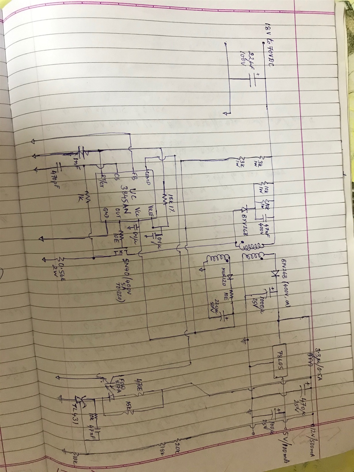
Hi, I have attached the schematic and transformer details of a UC3843 based power supply. 

However, when I power ON the SMPS with 20VC, there is no output .

Kindly advise a step by step procedure to see why he power supply is not starting.

For instance shall i check waveform at RtCt pin ? Also shall i check waveform at gate of MOSFET ?

What are the check points - Vcc, VREF, RtCt pin ??

Kindly advise

Regards

Atul BhakayTransformer details of Low Input DC and 6 output.docx
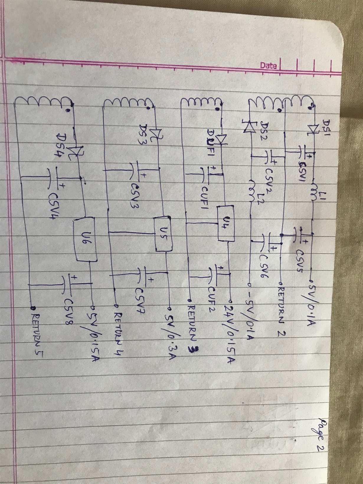
Transformer details of Low Input DC and 6 output.docx

  • Hi,

    schematic page 1 is also attached, now.

    Kindly advise on the schematic and how to get the smps started

    Regards

    Atul Bhakay

  • Hi Atul! 

    Thanks so much for reaching out and for your interest in the UC3843! For debugging, see steps below:

    1. Before applying input voltage, isolate the UC3843's VCC input and power it with a benchtop DC supply. Gradually raise the DC input on VCC and observe the UVLO threshold turn-on. You can check the signals at VCC, OUT, VREF, and RT/CT, verify proper VCC and expected VREF as well as PWM output at your desired frequency (set with RT/CT values). 
    2. Gradually begin applying DC input to the whole power stage. As you bring up the voltage, check to see that the FET is switching and check if you can observe a current sense waveform at Rsense (R6 in your schematic). 
    3. Does your IC start switching and then turn off again? This could be because your bootstrap circuit is taking too long to kick in and provide VCC, check the sizing of the bootstrap capacitor and the gap between UVLO ON and UVLO OFF on your chosen device. 
    4. Check the voltages on your secondaries and verify that they coincide with the transformer ratios as you designed. 
    5. Check for oscillation on the outputs as you raise the input voltage into your regulation range. Lots of oscillation can mean issues with your compensation loop or a need for an RC snubber on your output. 

    As you move through these steps, always be checking for excessive heat, odd smells, and smoke. 

    Thanks again for getting in touch, I hope this debug process helps get you started! 

    Aidan Davidson

  • Hi Aidan Davidson,

    Thanks for your prompt and detailed reply

    Yes, I will definitely follow the steps that you have suggested (the steps seem logical )

    I will revert if I have any further queries

    Regards

    Atul Bhakay

  • Hi Aidan Davidson,

    Continuing on this subject matter, kindly let me know if the UC384x schematic attached is OK or not.

    Specific queries :- a) Can pin 2 (VFB pin) be connected to ground as shown in schematic

    b) Comp pin connection (pin 1)  connection is also simplified by connecting directly to collector of opto-coupler. Is this ok ?

    In short, I am trying to keep things simple and yet get an effective, working DC to DC power supply

    Regards

    Atul Bhakay

  • Hi Atul! 

    Grounding the FB pin and tying the opto directly to the COMP pin is definitely a valid configuration! 

    Thanks for reaching out! 

    Aidan