- Ask a related questionWhat is a related question?A related question is a question created from another question. When the related question is created, it will be automatically linked to the original question.
Hello,
I am currently trying to design a step-down dc-dc converter with TPS54519.
The fact is that after reviewing the datasheet I am not able to design the compensation network.
I have seen a picture (Figure 28) in the datasheet that shows the open loop bode plot including both Filter output response and Modulator Gain.
The datasheet recommends using TINA-TI model TPS54519 to do so, but the model (SLVMBS8.TSC, TPS54519 TINA-TI Average Reference Design) shows the close loop response because a compensation network is required to be included in the circuit.
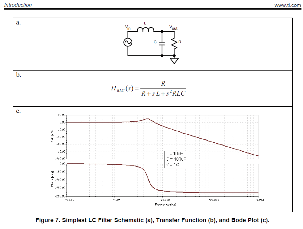
From my understanding and as far as I know and after confirming it in slva301.pdf document (see attached capture example for TPS40200D driver), I need output filter plus modulator gain to get the bode plot diagram and design the compensator network from this diagram. Output Filter (RLC) does not show the gain because is 1 (0dB) at low frequencies, obviously. (see attached RLC bode diagram example, slva301.pdf).
So, how can I get this (output filter plus modulator gain) bode plot diagram of the datasheet example (Figure 28)? What is the Modulator Gain of this TPS54519 driver?
Regards,