Because of the holidays, TI E2E™ design support forum responses will be delayed from Dec. 25 through Jan. 2. Thank you for your patience.

This thread has been locked.

If you have a related question, please click the "Ask a related question" button in the top right corner. The newly created question will be automatically linked to this question.

UCC21750: UCC21750 external RC for soft turn off (STO) with external BJT current buffer

Part Number: UCC21750

hello TI E2E

I have three big IGBT modules in parallel that are physically placed about 2 inches apart, because the size of IGBT modules are large.

Each IGBT modules has two IGBTs in half-bridge configuration.  And each IGBT has its own local BJT buffer.

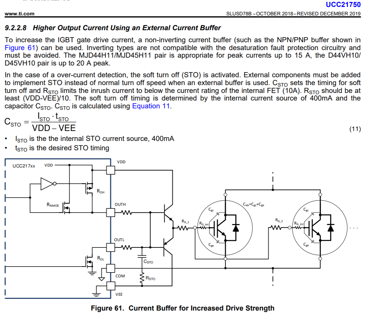
I have a question about the external R and C for soft turn off (STO). that are shown in Fig. 61 on page 45 in the datasheet.

I attached a few captures from datasheet here for easy communication. 

Q1: Shall I put a single pair of RC close to UCC21750 to soft turn off all IGBTs' BJT buffers?  OR I should put distributed parallel pairs of RC (reduced value by # of pairs) close to each BJT buffer as close as possible.

The reason I am asking is that I found some Vge ringing during STO which is triggered by Desat fault. The debugging is still in progress. I didn't post any oscilloscope capture here yet.

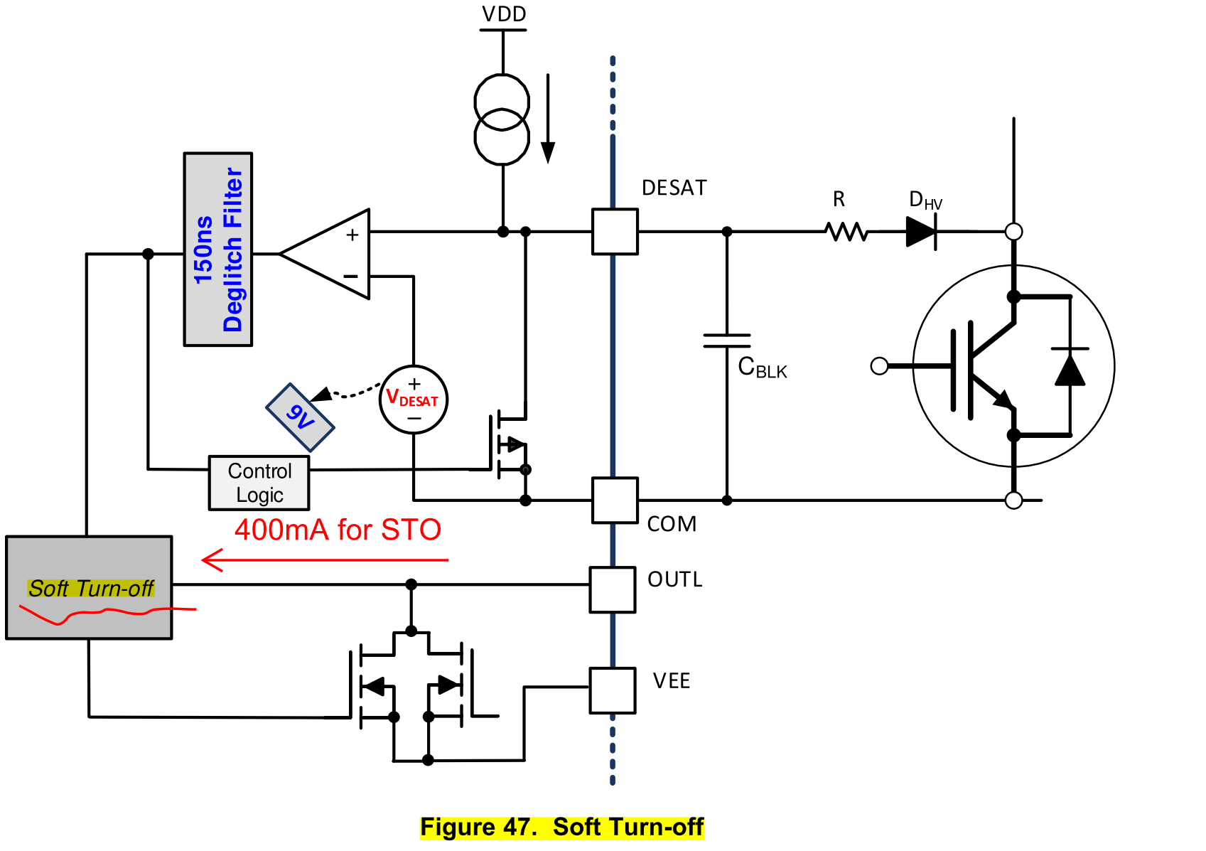
Q2: What are the purposes of the two back-to-back MOSFETs for in Fig.47 on page 31?  Could you explain it to me? 

Any insights into external RC for STO will be much appreciated.

Thank you.

YZ

  • I just realize this is a new thread that should be disconnected from another thread of "UCC21750: Simulation with LTSpice". 

  • Hi Yee, Thanks very much for your detailed questions.

    May I know which is your current schematic design? single pair or double pair? do you have some existing scope shots to share the performance of current setup? or you are studying to prepare the schematic for paralleled IGBTs?

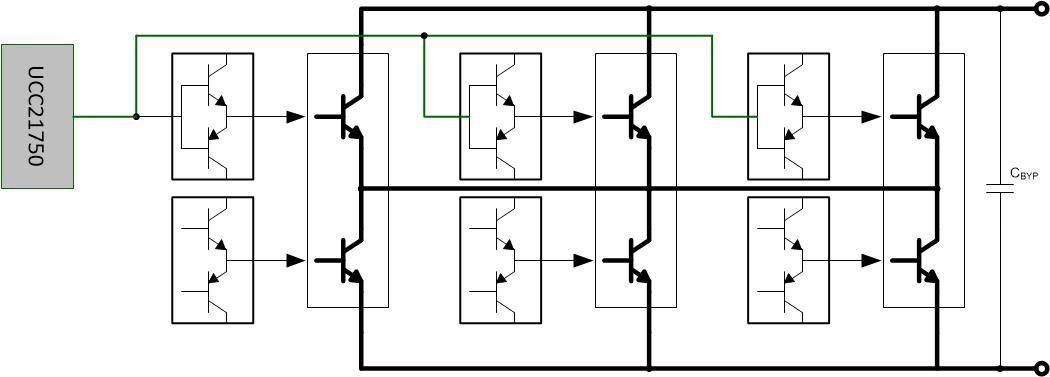
    I created a drawing below, does it reflect your current power stage and gate driver design, can you please confirm?

  • Wei

    I am testing the circuits on bench now. I am driving 3 IGBT modules in parallel using single UCC21750 to give high current capability. 

    I am still investigating this right now. But I would like to know more about the distributed external RC for BJT buffers.

    Please see my illustration below. 

    Thanks

    YZ

  • YZ, thanks a lot for your quick feedback. Can you please check and confirm my drawing? it was not uploaded correct in my first submission. I have Gangyao, an expert in my team, will reply with more details.

  • Can you see my drawing and give me some comments?

    I found that the high dv/dt on gate signal may causing additional ringing problems. 

    In my case, there are 3 big IGBT modules in parallel to give >1kA peak current.

  • Hi Yee,

    Could you post a Vge ringing waveform during the STO? As the total UCC21750 OUTL sink current will be 400mA during STO, I am wondering are there good current sharing between these three branches of turn off circuit? So I would suggest you to try the test with just use one RSTO + CSTO for all the three IGBTs.

    Regards,

    Gangyao

  • hi Gangyao

    Thanks for your reply. It seems the problem is solved by adding a RC of STO at the most suspicious IGBT buffer. The ringing during STO is gone. I believe it is related to my layout and the signal integrity since the high dv/dt.

    Finally, I put additional RC pairs at other IGBT buffers. It serves as a RC termination as well at local current Buffers.

    Please give me your email address. I can send you a few scope captures and discuss about it in details.

    This is just the beginning of the bench test without any high voltage switching. Next, I will move to high voltage switching test (e.g., double pulse)

    * We are driving 3xIGBT modules in parallel to have >1200A peak current.

    Thank you.

    YZ