This thread has been locked.

If you have a related question, please click the "Ask a related question" button in the top right corner. The newly created question will be automatically linked to this question.

BQ2057W: Device Diagram Issue Consult

Part Number: BQ2057W

Hi TI expert,

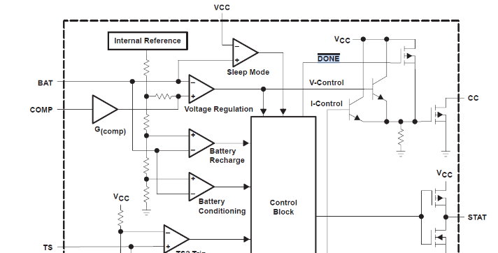
Could you please analysis the details of two issue points in the device diagram:

1. How does the DONE signal (low effective) stop the charge process?

2. How can output CC pin with a P-channel MOSFET turn on and regulate the current?

Thanks.

B R,

Jayce L

  • Hi Jayce,

    How does the DONE signal (low effective) stop the charge process?


    When the /DONE signal is pulled low, it drives the gat eof a P-Type FET. That FET is now closed and allows for VCC to flow to the CC MOSFET. The MOSFET is the analog path that controls conduction at the CC pin . The current into the CC pin will control the external BJT or MOSFET. 

    How can output CC pin with a P-channel MOSFET turn on and regulate the current?


    The CC is operating as a current source to control the external BJT/MOSFET. 

    Please note that this is a functional representation and may not be the exact representation of the internal circuit. Please let me know if there are any application problems.