This thread has been locked.

If you have a related question, please click the "Ask a related question" button in the top right corner. The newly created question will be automatically linked to this question.

TPS40305: Issue with transient current

Part Number: TPS40305

Hi

I use the evm sample and design my own board, but I have issue with output voltage which does not stabilize after input transient voltage or current. you can see in below graph the voltage stay off until high current  or transient voltage turn off. When you compare this with webbench simulation does not match. I am not sure what I am doing wrong.

Web Bench simulation

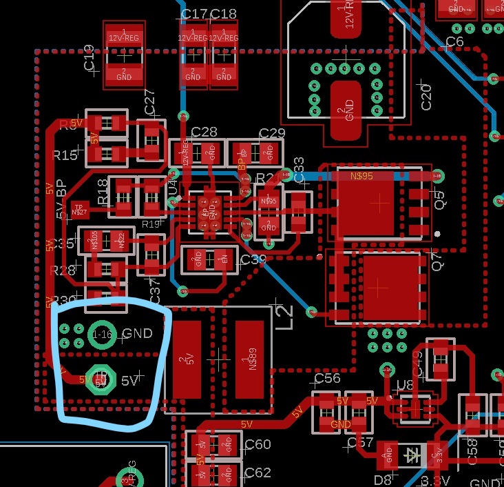
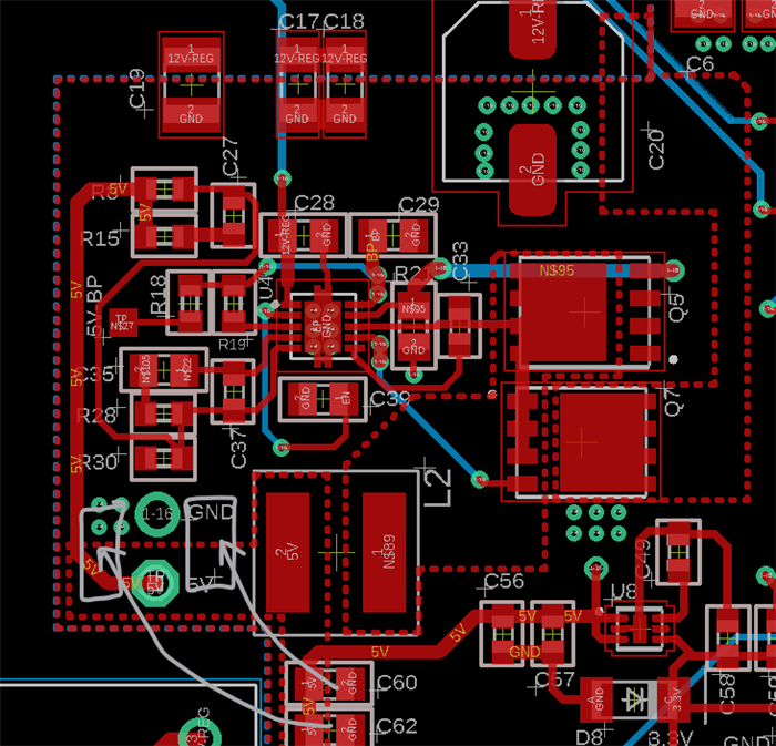
Below is my schematic and footprint

Please let me know if you have any quesitons.

Thank you

  •  

    The 50mV shift in the output voltage loops pretty sizable, but there are a couple of possibilities:

    1) Do you have multiple oscilloscope probes on the same oscilloscope connected to different ground terminals on your board?

    Oscilloscopes typically use a common input ground "bus-bar" that is also connected to earth ground through their grounded AC power plug.  When passive probes are connected to different ground points on the same PBC, there is more resistance in the ground shield of the oscilloscope probes cables than then between the ground terminals of the probes.  If the load current applied during the test causes a ground-drop on the board, the two Oscilloscope probes will divide the difference between the ground points, then multiply the difference by a 10x factor when they cancel the passive probe-tip attenuator.  That can allow a 5mV ground drop within the design to appear as a 50mV output voltage change.

    2) Where are you measuring VOUT in relation to were VOUT connects into the feedback path going to R8 and where you are drawing current out of VOUT? 

    The TPS40305 is actually regulating the voltage at the FB pin (between R8 and R30) to match its 0.600V reference.  If there is additional voltage drop between the inductor's output and the feedback regulation point, after the point where you are monitoring Vout with the oscilloscope, the resistive drop between the Oscilloscope monitored output voltage and the Feedback monitored output voltage would appear as a DC rise in VOUT like this.

    3) What is the voltage at the ground terminal of R30 with respect to the GND pin of the TPS30405?

    Since the TPS40305 is regulating the voltage at it's FB pin relative to it's GND pin, voltage differences between the ground voltage on R30 (FB to GND resistor) and the ground of the TPS4035 can create a DC regulation offset like this.  6mV at the GND pin will produce a 1% shift in VOUT.  Consistent with the 50mV you are seeing.

  • Hi Peter,

    Thanks for the quick reply. I try to answer your questions as best as I can, please let me know if my answer was not suffusion. 

    1.  I am using single ground for reading 5V output. 

    2. I think above image will answer your question but below is measuring voltage right on R8, pin and other side of board, using ground close to the ground mark above. The noisy area is where relay turns on but no load on 5v Relay only on 12V supply which feed to 5V regualtor.

    3. The voltage between ground point ot R8 ground is 0.596V

    I also Attached the Gerber file for  your information. Please let me know if you need any thing else.

    A-1300-X07.zip

    Thank you

  •   

    Perhaps I am I missing something, but it appears to me that the waveform you posted as "PIN" above is not showing the 50mV DC shift in the output voltage when under load.  Is there some other issue that you are looking at and need assistance solving?

  • Hi

    Maybe I have to put my question in another way when have input transient voltage  you can see output of regulqtor become alot noiser and lift depend on position.

    Thank you

  •  

    Ok, to better understand the increased AC "noise" we'll need a better resolution oscilloscope waveform of the output voltage ripple, something taken at 2us/division or 5us/division so we can see the shape of the output voltage ripple.

    If we are seeing 1 AC ripple at 1.2MHz switching frequency with another, lower frequency ripple changing the cycle by cycle average, we may be looking at a compensation loop stability problem.

    If, on the other hand, the increased AC ripple is high frequency spikes at the switch transition points within the ripple, then we are either looking at an issue with the high-frequency bypassing of the output (excessive ESR/ESL, Trace inductance, etc), coupling of switch node switch transition ringing from the SW node to the output, or high-frequency coupling pick-up from the oscilloscope probe.

    To minimize the later, we will typically remove the plastic jacket from the oscilloscope probe wrap a bare "bus" wire around the exposed metal ground barrel of the probe tip, and then connect that to the ground terminal of one of the output capacitors (with just pressure) and the oscilloscope probe top to the other terminal.

    To help with the prior two, we can look at modifications to reduce the switch-node ringing, and if any improvements can be made to the output voltage decoupling capacitors.

  •  

    I am glad to see that we have resolved your issue.  If you don't mind, for my information, and for anyone searching this issue in the future, what was the resolution?

    Do you still need me to review the compensation design from your schematic?

    And is there any more assistance I can offer?

  • Hi

    Unfortunately the issue is not solved, I accidently press the solved button instead of reply. I am waiting to go to office tomorrow so I can send you some more pictures. 

    I believe the issue maybe is due ground bouncing or AC couple as you mentioned.

    Thank you

  •  

    Unfortunately, I do not see a way to remove the "resolved" tag from the thread.

    Let's take a look at those measurements, and I will also check the loop design stability. 

    Is the only VOUT to GROUND bypassing C60 and C62?

    How are the ground terminals of C60 and C62 routed back to the output ground for 1-16, the source of Q5, and the GND pad of the TPS40305?  I do not see any via or through-holes noted near their ground terminals.

  • Hi Peter,

    Thanks again for replying super fast.  Yes C60 C62 is my output  bypass capacitor which is two 22uF C0805X5R160-226KNE.

    Regarding ground I have ground plane on top and bottom which it connect to each other. There is J6 connector hole  which connect to bottom layer.

    Please let me know if you have any questions.

  •  

    The AC ripple current in the C60 and C62 bypass capacitors needs to flow from their ground terminals to the Source terminal of the sychronous FET and to the ground terminal of the input capacitor.  WIth no vias near C60 and C62 or the source pins of Q5 (synchronous FET) and no top-layer path between these points, it is hard to visualize the AC current path.  High AC impedance between the bypass capacitors and the synchronous FETs could compromise the loop stability, and add significant high-frequency noise.

    Some additional things to try:

    1) Solder a piece of copper braid (solder wick) or stranded wire (thicker the better) between the ground terminals of C60 / C62 and the source pins of the Synchronous FET (Q5) to see if that reduces the noise by improving the grounding.

    2) scratch off some of the solder mask at the output voltage and ground by the through holes, and move C60 AND C62 closer to the through holes where there are ground vias to the bottom layer.

  • HI Peter,

    I agree I need improve the grounding that's why I am re-layout the board. I have tired you suggestion number one and below is the result.

    Remember there is only 30mA of load (Relay) is on this regulator. I believe the ground is bouncing up and down when you turn on relay.  Also on my previous board I had C60,C62 and that location you mentioned buy same result. 

    Thank you

  • Hi Amir

        Do you have further questions on this issue?

    regards,

    Gerold

  • Hi Gerold,

    I have issue with this 5v regulator that is very noisy and voltage drop on transient voltage. Take look at below graph which show 12V input and 5V out of regulator. you can see when relay turns on and put load on 12V supply which is around 2.5A nothing happen on 12V but on 5V which is turning on relay is all noisy.

  •  

    Your prior message shows that after adding ground connection from your output capacitor ground to your synchronous rectifier ground has less than 5mV peak to peak ripple and less than 5mV shift under load, based on the scale on the left of the image.

    Does your application require less ripple than that?

    Do you need guidance in how to update the layout based on that test result?

    Or maybe I am misinterpreting the results you shared, and you are still seeing a large output ripple and voltage shift?

    Additionally, part of your e-mail describes 2.5A and part 30mA..  What is the load that the TPS40305 converter is driving?  30mA is a pretty low current for a power converter running with the TPS40305 controller, if you only need 30mA at 5V, we would likely be able to offer a more optimized solution.

  • Hi Peter,

    I will be appreciate if you can give us some suggestion on layout  so we have better result  on next revision of board. Less ripple always is better for us since are logic section of our board is powered through this regulator. I convert 5V out put to 3.3V using linear regulator to reduce ripple.

    The load I will run on TPS40305 is around 2A but in this test was only running around 530mA. What I meant on my previous comment was that this happen only when relay turns on which consume only 30mA (That relay rated for)  

    Thank you

  • So, you only see this noise when you turn on the relay, but not when there are other loads on the output?

    Is this a mechanical / magnetic relay, or a solid-state relay?

  • Hi Peter,

    Yes that is true when I turn rely or when the screen backlight turns on and off. 

    Relay is mechanic G5Q-1A4DC5

    Can this be all due to ground issue.

    Thank you

  • Amir,

    It would be the inductive nature of the relay.

    I will take a look at the compensation later today and see if I notice anything.

  •   

    I took a look at the compensation.  It is certainly conservative for a 1.2MHz switcher, but I don't see any issue.  I have attached the Excel spreadsheet with the loop analysis.  TPS40KType III Loop Stability kVenable_TPS40305.xls

    So, I think the primary concern / issue is the ground inductance due to long return loops between the output capacitors and the source of the synchronous rectifier, and the input capacitor. 

    What does the stack-up of the PCB look like?  Do you have internal ground planes, or just signal layers, or a 2-layer board?

  • Hi Peter,

    On Current PCB I only have two layer board (Ground on top and bottom), but new 4 layer board   that I am designing I have gnd on top and 2nd layer as you can see on below image

    Part positioning exactly like EVM board

    Top Ground PLANE

     2ND layer is GND PLAN everywhere with no traces

    Layer 3 and bottom there is 12V plan


    Do you think this will work or I need to remove 12V plane. Also let me know I if you have any other questions or comment.

    Thank you

  •  

    I think this will work much better for you.  One recommendation, on the vias around the capacitor terminals, spread the vias out slightly so that the copper pours on the internal layers that are not connected to them can flow between the vias and not be cut/slotted.  That will significantly improve the current flow and reduce the inductance over a slot.

  • Hi Peter,

    Thanks for reply, I will go a head and give more spacing between my vias as you mentioned. I will update you as soon I get the new board.

    Thanks for all you help and have a great holidays. 

    Amir

  •   

    Have a wonderful, and safe Holidays Amir.  I will close our this thread, if you have any additional questions, let's start a new thread.