This thread has been locked.

If you have a related question, please click the "Ask a related question" button in the top right corner. The newly created question will be automatically linked to this question.

LM7480-Q1: 48V Automotive rail protection (in addition to 12V and 24V rails)

Part Number: LM7480-Q1
Other Parts Discussed in Thread: LM7480, LM74800-Q1

Hi,

I am planning on using the LM7480-Q1 for a device that can work on automotive 12V rail, 24V rail and 48V rail. 

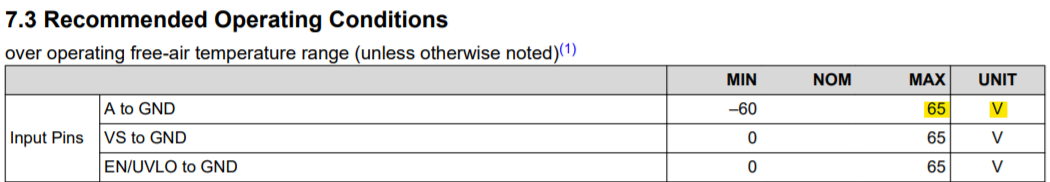
If I combine the requirements for ISO16750 and ISO21780, I have a wide input voltage range = 6V to 58V, in which I need to pass with ClassA rating.

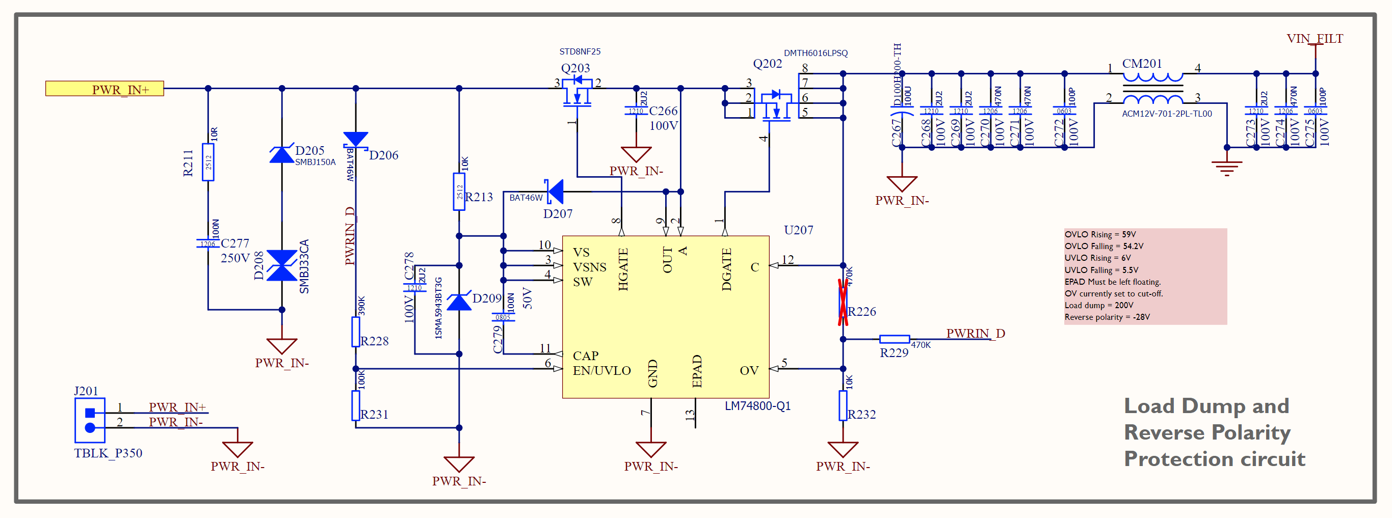
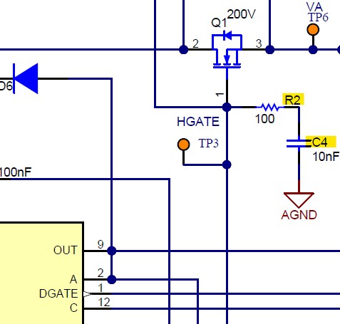
Is it possible to set the LM7480-Q1 to work at this voltage range? i.e. UVLO set to 6V, OV set to 58V? Can I connect in common-source topology as described in 9.5.2 of datasheet 

Datasheet link: https://www.ti.com/lit/gpn/lm7480-q1

This means that voltage at HGATE and DGATE (with respect to GND) must be greater than voltage at A and OUT, i.e. >58V. Is this possible? What is the max rating of the charge pump output?

If this is not possible could you please suggest another part that can work with all three 12V, 24V and 48V rails and help suppress load dumps, reverse polarity and transients?

Thanks in advance

Navin

  • Hi Navin,

    What is the Max voltage (in all conditions including conditions like load dump) that we can expect on 48V rail in your system ?

    LM7480-Q1 can be used if the Max Operating voltage is less than 65V (Recommended Operating Voltage).

    The HGATE and DGATE and are generated internally w.r.t OUT and A respectively. Their voltages shouldn't be a problem as long as the voltage n A, VS are within the Recommended Operating Conditions.

  • Hi Praveen

    The max positive transient will be 202V (ISO16750-2:4.6.4 Load dump). If I use circuit as shown below (Fig 10-25 in LM7480 datasheet):

    • D3 will clamp anything >150V. 
    • D4 will clamp any negative pulse <-33V.
    • D1 will protect VS pin from any voltage >60V
    • What is the purpose of D2? Is it to prevent OUT and A being <Vs? 

    Thanks for confirming that HGATE and DGATE wil be generated internally, with ref to OUT

  • Hi Praveen

    Thanks for confirming the HGATE and DGATE voltages.

    The max voltage on the input rail is 204V (ISO16750-2:4.6.4 Load dump) so I was thinking of using this circuit below (fig 10-25 in datasheet), Please confirm the below:

    • D3 clamps all voltages >150V
    • D4 clamps all negative pulses <-33V
    • D1 limits voltage at Vs to 60V
    • What is the purpose of D2? Is it to prevent OUT and A to be a lower voltage than VS? Or is it some protection?

    Thanks in advance

  • Hi Navin,

    Yes, The common-source topology shown in Figure 10-25 of datasheet can withstand  200-V Unsuppressed Load Dump. Please see my response below,

    • D3 clamps all voltages >150V
      • D3+D4 clamps the voltage at Input to less than 200V so as to not exceed the VDS rating of the 200V FET. 
    • D4 clamps all negative pulses <-33V
      • Yes, this is to make sure the -ve voltage seen by the controller is within its Abs max rating of the controller (-65V).
    • D1 limits voltage at Vs to 60V
      • Yes, this is to limit the voltage on VS pin in all conditions to be within the Abs Max Rating of VS pin (70V).
    • What is the purpose of D2? Is it to prevent OUT and A to be a lower voltage than VS? Or is it some protection?
      • The purpose of D2 is to supply voltage to the VS pin from A pin. The 10 kohms in series with VS pin (which is placed to limit the current into Zener) limits the current required by the charge pump during startup conditions. So, a diode from A to VS provides uninterrupted current into the VS pin. 

  • Hi Praveen

    Thanks for the answers

    You mentioned the below


    Praveen GD said:

    The purpose of D2 is to supply voltage to the VS pin from A pin. The 10 kohms in series with VS pin (which is placed to limit the current into Zener) limits the current required by the charge pump during startup conditions. So, a diode from A to VS provides uninterrupted current into the VS pin. 

    If there is a cold crank (undervoltage) or negative transient pulse, then Vs will be interrupted, does this mean that Ca will discharge and current flows through D2 and into Vs? In what other situations will the current to Vs be interrupted?  

    I am working on the schematic for this, which I will post in the next post, would you be able to review it for me? Thanks in advance

    Thanks

    Navin

  • Hi Navin,

    Without D2, the charge pump may not build up to the full capacity. The diode D2 provides a low impedance path (bypassing the 10k resistor) for power supply of the chip. This is valid in  normal conditions as well. 

    Yes, you can send the schematic for review once it is done.  

  • Hi Praveen

    Thanks for the confirmation, D2 makes sense now. Please find schematic attached, could you please review for me?

    Thank you very much in advance

  • Hi Navin,

    Thanks for sharing the schematics. I will review and get back to you by coming Tuesday. 

  • Hi Navin,

    The LM74800-Q1 schematics look good to me. 

    You can add a R and C in series from HGATE to GND (as shown below) and keep them at DNP. The RC may be useful in case you would like to have a dv/dt start up sometime later.

  • Hi Praveen

    Thanks for your reply, much appreciated. Thanks for confirming schematic.

    Regarding the soft-start, please confirm if R2 needs to be 0603 and C4 needs to be 100V rated?

    Thanks

    Navin

  • Hi Navin,

    R2 can be 0603 or 0402. There will be power dissipation across it only during startup and turn off. 

    C4 needs to be rated for > [Vin(max) + 15V]

  • Hi Praveen

    Very much appreciate your help in this matter, I will use this schematic

    Thanks

    Navin